System Debug
11-8 Copyright © 2005-2008 ARM Limited. All rights reserved. ARM DDI 0337G
Non-Confidential
Unrestricted Access
Flash Patch Control Register
Use the Flash Patch Control Register to enable the flash patch block.
The register address, access type, and Reset state are:
Address
0xE0002000
Access Read/write
Reset state Bit [0] (ENABLE) is reset to 1'b0.
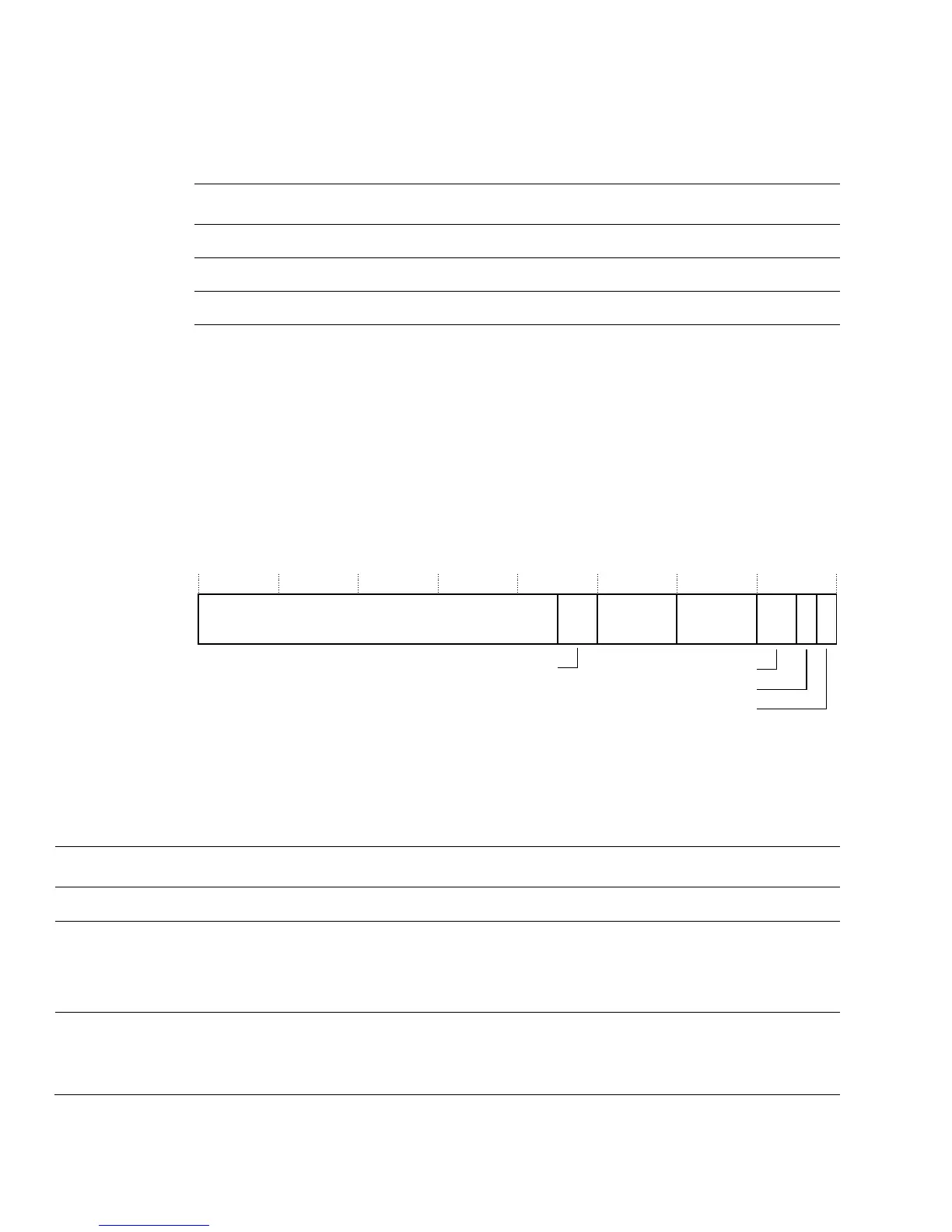
Figure 11-2 shows the bit assignments of the Flash Patch Control Register.
Figure 11-2 Flash Patch Control Register bit assignments
Table 11-2 describes the bit assignments of the Flash Patch Control Register.
CID1 Read-only
0xE0002FF4
Val ue
0xE0
CID2 Read-only
0xE0002FF8
Val ue
0x05
CID3 Read-only
0xE0002FFC
Val ue
0xB1
Table 11-1 FPB register summary (continued)
Name Type Address Description
31 3 2 1 0
Reserved
12 478
NUM_LIT
NUM_CODE1
ENABLE
1114 13
NUM_CODE2
KEY
Reserved
Table 11-2 Flash Patch Control Register bit assignments
Bits Field Function
[31:15] - Reserved. Read As Zero. Write Ignored.
[14:12] NUM_CODE2 Number of full banks of code comparators, sixteen comparators per bank. Where less than
sixteen code comparators are provided, the bank count is zero, and the number present
indicated by NUM_CODE. This read only field contains 3'b000 to indicate 0 banks for
Cortex-M3 processor.
[11:8] NUM_LIT Number of literal slots field. This read only field contains either b0000 to indicate there are
no literal slots or b0010 to indicate that there are two literal slots.