Trace Port Interface Unit
ARM DDI 0337G Copyright © 2005-2008 ARM Limited. All rights reserved. 17-19
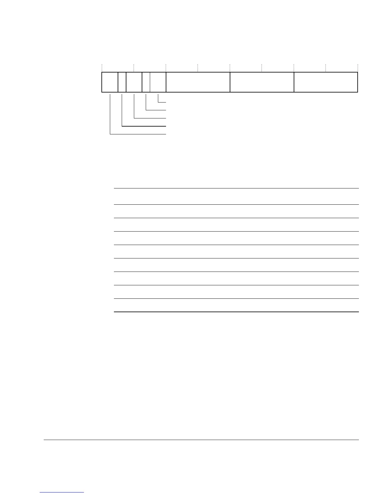
Figure 17-13 Integration register : FIFO data 1 bit assignments
Table 17-15 lists the bit assignments of the Integration register : FIFO data 0.
CoreSight specific registers
This section describes the CoreSight specific registers.
Claim Tag Clear Register
The register address, access type, and Reset state are:
Address
0xE0040FA4
Access Read/write
Reset state
0x0
This register forms one half of the Claim Tag value. This location enables individual bits
to be cleared, write, and returns the current Claim Tag value, read.
FIFO2 data 2 FIFO2 data 1
FIFO2 data 0
31 0
29 2728 26
2425 23
16
15
87
Write point 1
ATVALID1S
Write point 2
ATVALID2S
30
Reserved
Table 17-15 Integration register : FIFO data 1 bit assignments
Bits Field Function
[31:30] - Reserved
[29] ATVALID2S
[28:27] Write point 2
[26] ATVALID1S
[25:24] Write point 1
[23:16] FIFO2 data 2
[15:8] FIFO2 data 1
[7:0] FIFO2 data 0