System Debug
11-16 Copyright © 2005-2008 ARM Limited. All rights reserved. ARM DDI 0337G
Non-Confidential
Unrestricted Access
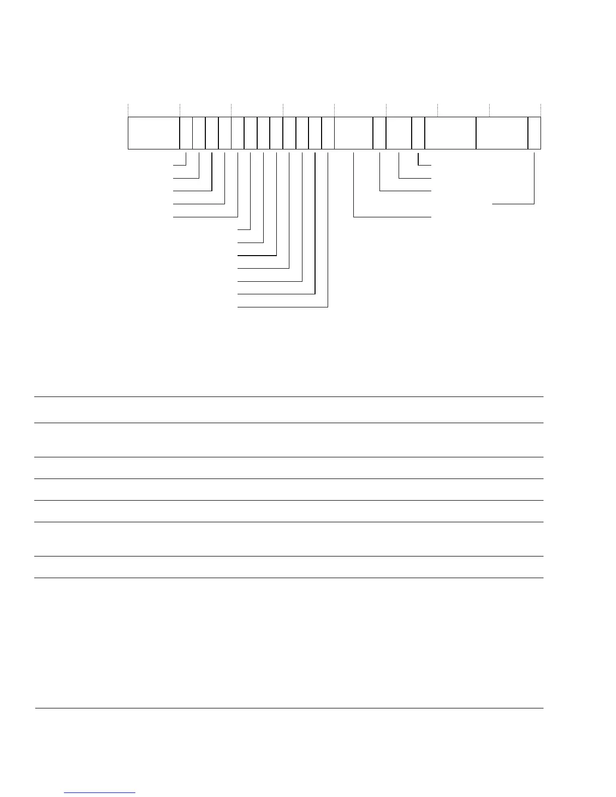
Figure 11-5 DWT Control Register bit assignments
Table 11-7 describes the bit assignments of the DWT Control Register.
31 019 18 17 16 15 13 12 11 10 8 5
POSTCNT POSTPRESET
28 27
NUMCOMP
SLEEPEVTENA
EXCEVTENA
CPIEVTENA
EXCTRCENA
PCSAMPLENA
SYNCTAP
202122
CYCEVTENA
FOLDEVTENA
LSUEVTENA
1
4
9
CYCCNTENA
CYCTAP
23
NOEXTTRIG
NOTRCPKT
242526
NOCYCCNT
NOPRFCNT
Reserved
Reserved
Table 11-7 DWT Control Register bit assignments
Bits Field Function
[31:28] NUMCOMP Number of comparators field. This read-only field contains the number of comparators
present. Valid values are b0100, b0001, or b0000.
[27] NOTRCPKT When set, trace sampling and exception tracing are not supported.
[26] NOEXTTRIG When set, no CMPMATCH[N] support.
[25] NOCYCCNT When set, DWT_CYCCNT is not supported.
[24] NOPRFCNT When set, DWT_FOLDCNT, DWT_LSUCNT, DWT_SLEEPCNT, DWT_EXCCNT, and
DWT_CPICNT are not supported.
[23] Reserved -
[22] CYCEVTENA Enables Cycle count event. Emits an event when the POSTCNT counter triggers it. See
CYCTAP (bit [9]) and POSTPRESET, bits [4:1], for details.
1 = Cycle count events enabled
0 = Cycle count events disabled.
This event is only emitted if PCSAMPLENA, bit [12], is disabled.
PCSAMPLENA overrides the setting of this bit.
Reset clears the CYCEVTENA bit.