Preface
ARM DDI 0337G Copyright © 2005-2008 ARM Limited. All rights reserved. xxiii
Unrestricted Access Non-Confidential
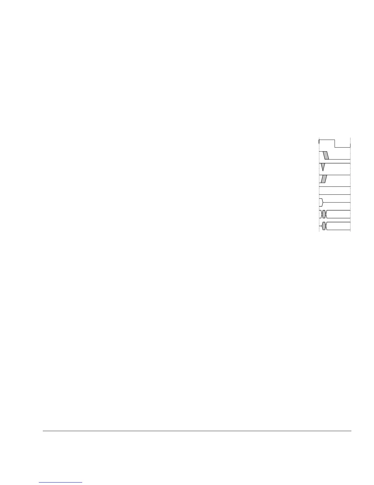
Timing diagrams
The figure named Key to timing diagram conventions explains the components used in
timing diagrams. Variations, when they occur, have clear labels. You must not assume
any timing information that is not explicit in the diagrams.
Shaded bus and signal areas are undefined, so the bus or signal can assume any value
within the shaded area at that time. The actual level is unimportant and does not affect
normal operation.
Key to timing diagram conventions
Signals
The signal conventions are:
Signal level The level of an asserted signal depends on whether the signal is
active-HIGH or active-LOW. Asserted means:
• HIGH for active-HIGH signals
• LOW for active-LOW signals.
Lower-case n At the start or end of a signal name denotes an active-LOW signal.
Prefix A Denotes global Advanced eXtensible Interface (AXI) signals.
Prefix AR Denotes AXI read address channel signals.
Prefix AW Denotes AXI write address channel signals.
Prefix B Denotes AXI write response channel signals.
Prefix C Denotes AXI low-power interface signals.
Prefix H Denotes Advanced High-performance Bus (AHB) signals.
Clock
HIGH to LOW
Transient
HIGH/LOW to HIGH
Bus stable
Bus to high impedance
Bus change
High impedance to stable bus