Virtex-5 FPGA User Guide www.xilinx.com 101
UG190 (v5.0) June 19, 2009
General Usage Description
PLLs in the bottom half of the Virtex-5 device are driven by the global clock pins in bank4
and can be paired as listed in Table 3-6.
Other important notes on these pairings:
• The pin description names do not contain other possible multipurpose functions such
as _CC, _VRN, _VRP or _VREF.
• Only the P-side pins are shown. For differential clock connections use the equivalent
N-side pin. Inside the FPGA, only the P-side of the differential pin pair can connect to
the CMT.
• For a mapping to the actual pin numbers consult the Virtex-5 Family Packaging
Specifications.
PLL Clock Input Signals
The PLL clock source can come from several sources including:
• IBUFG - Global clock input buffer, the PLL will compensate the delay of this path.
• BUFGCTRL - Internal global clock buffer, the PLL will not compensate the delay of
this path.
• IBUF - Not recommended since the PLL can not compensate for the delay of the
general route. An IBUF clock input must route to a BUFG before routing to a PLL.
• DCMOUT - Any DCM output to PLL will compensate the delay of this path.
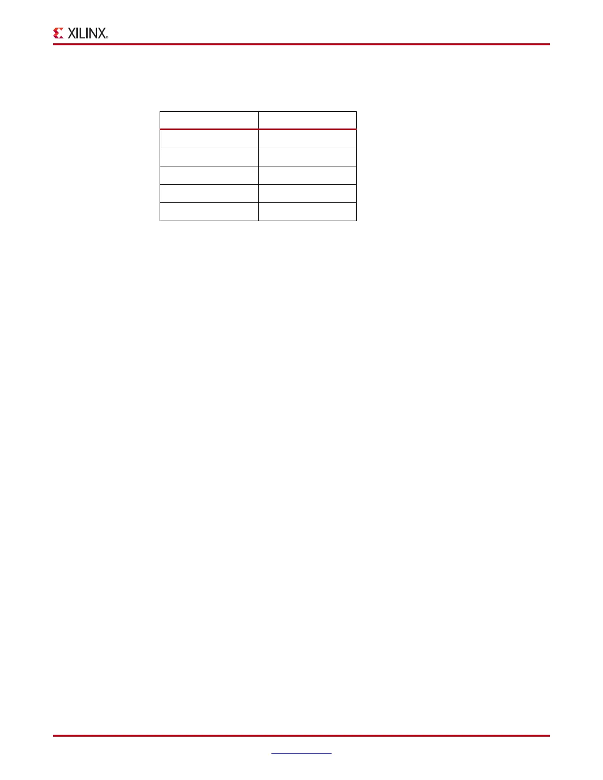
Table 3-7: PLLs in the Bottom Half Pairing
CLKIN1 CLKIN2
IO_L9P_GC_4 IO_L4P_GC_4
IO_L8P_GC_4 IO_L3P_GC_4
IO_L7P_GC_4 IO_L2P_GC_4
IO_L6P_GC_4 IO_L1P_GC_4
IO_L5P_GC_4 IO_L0P_GC_4
 Loading...


