368 www.xilinx.com Virtex-5 FPGA User Guide
UG190 (v5.0) June 19, 2009
Chapter 8: Advanced SelectIO Logic Resources
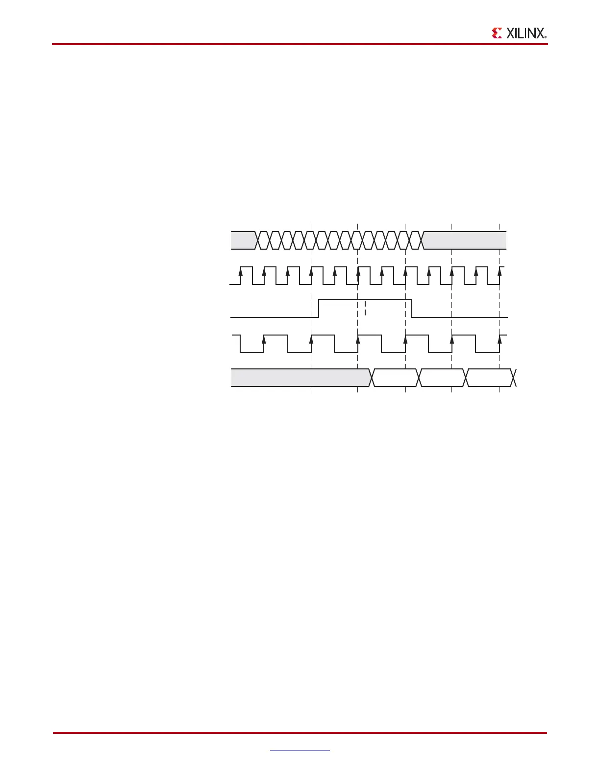
Bitslip Timing Model and Parameters
This section discusses the timing models associated with the Bitslip controller in a 1:4 DDR
configuration. Data (D) is a repeating, 4-bit training pattern ABCD. ABCD could appear at
the parallel outputs Q1–Q4 of the ISERDES in four possible ways: ABCD, BCDA, CDAB,
and DABC. Only one of these four alignments of the parallel word makes sense to the
user's downstream logic that reads the data from the Q1–Q4 outputs of the ISERDES. In
this case, ABCD is assumed to be the word alignment that makes sense. Asserting Bitslip
allows the user to see all possible configurations of ABCD and then choose the expected
alignment (ABCD). Figure 8-12 shows the timing of two Bitslip operations and the
corresponding re-alignments of the ISERDES parallel outputs Q1–Q4.
Clock Event 1
The entire first word CDAB has been sampled into the input side registers of the ISERDES.
The Bitslip pin is not asserted; the word propagates through the ISERDES without any
realignment.
Clock Event 2
The second word CDAB has been sampled into the input side registers of the ISERDES.
The Bitslip pin is asserted, which causes the Bitslip controller to shift all bits internally by
one bit to the right.
Clock Event 3
The third word CDAB has been sampled into the input side registers of the ISERDES. The
Bitslip pin is asserted for a second time, which causes the Bitslip controller to shift all bits
internally by three bits to the left.
On this same edge of CLKDIV, the first word sampled is presented to Q1–Q4 without any
realignment. The actual bits from the input stream that appear at the Q1–Q4 outputs
during this cycle are shown in A of Figure 8-13.
X-Ref Target - Figure 8-12
Figure 8-12: Bitslip Timing Diagram
ug190_8_12_100307
CD ABCD CDABCDAB
CLK
BITSLIP
CLKDIV
D
12
Bitslip1 Bitslip2
435
Q4–Q1
CDAB BCDA ABCD
 Loading...


