Virtex-5 FPGA User Guide www.xilinx.com 123
UG190 (v5.0) June 19, 2009
Block RAM Library Primitives
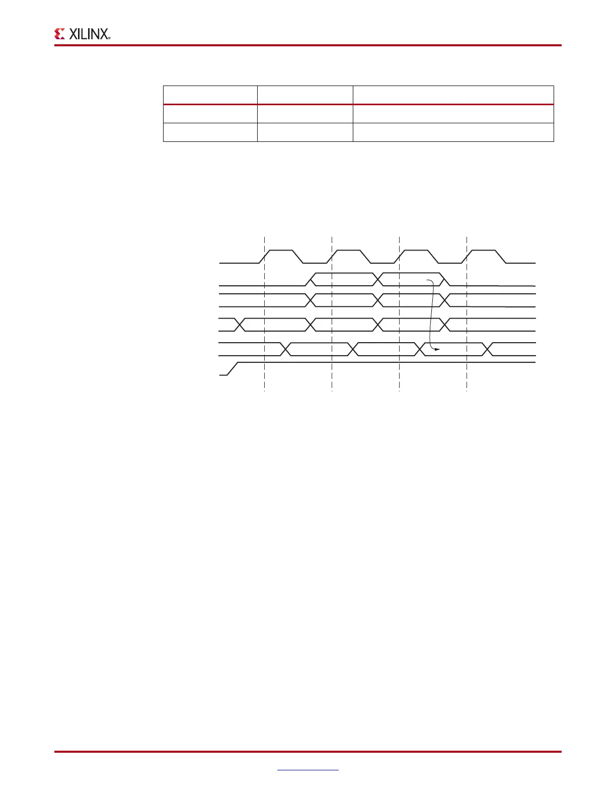
When the RAMB36 is configured for a 36-bit or 18-bit wide data path, any port can restrict
writing to specified byte locations within the data word. If configured in READ_FIRST
mode, the DO bus shows the previous content of the whole addressed word. In
WRITE_FIRST mode, DO shows a combination of the newly written enabled byte(s), and
the initial memory contents of the unwritten bytes.
Block RAM Error Correction Code
Both block RAM and FIFO implementations of the 36 Kb block RAM support a 64-bit Error
Correction Code (ECC) implementation. The code is used to detect single and double-bit
errors in block RAM data read out. Single-bit errors are then corrected in the output data.
Block RAM Library Primitives
The Virtex-5 FPGA block RAM library primitives, RAMB18 and RAMB36, are the basic
building blocks for all block RAM configurations. Other block RAM primitives and macros
are based on these primitives. Some block RAM attributes can only be configured using
one of these primitives (e.g., pipeline register, cascade, etc.). See the “Block RAM
Attributes” section.
The input and output data buses are represented by two buses for 9-bit width (8 + 1), 18-bit
width (16 + 2), and 36-bit width (32 + 4) configurations. The ninth bit associated with each
byte can store parity/error correction bits or serve as additional data bits. No specific
function is performed on the ninth bit. The separate bus for parity bits facilitates some
designs. However, other designs safely use a 9-bit, 18-bit, or 36-bit bus by merging the
regular data bus with the parity bus. Read/write and storage operations are identical for
all bits, including the parity bits.
RAMB18 18 2
RAMB18SDP 36 4
X-Ref Target - Figure 4-8
Figure 4-8: Byte-wide Write Operation Waveforms (x36 WRITE_FIRST)
Table 4-4: Available Byte-wide Write Enables (Continued)
Primitive Maximum Bit Width Number of Byte-wide Write Enables
CLK
WE
DI
ADDR
DO
EN
Disabled Read
XXXX 1111 2222
1111 0011
XXXX
aa bb bb cc
0000 MEM(aa) 1111 1122 MEM(cc)
ReadWrite
MEM(bb)=1111
Byte Write
MEM(bb)=1122
ug190_4_10_032106
 Loading...


