Virtex-5 FPGA User Guide www.xilinx.com 229
UG190 (v5.0) June 19, 2009
SelectIO Resources General Guidelines
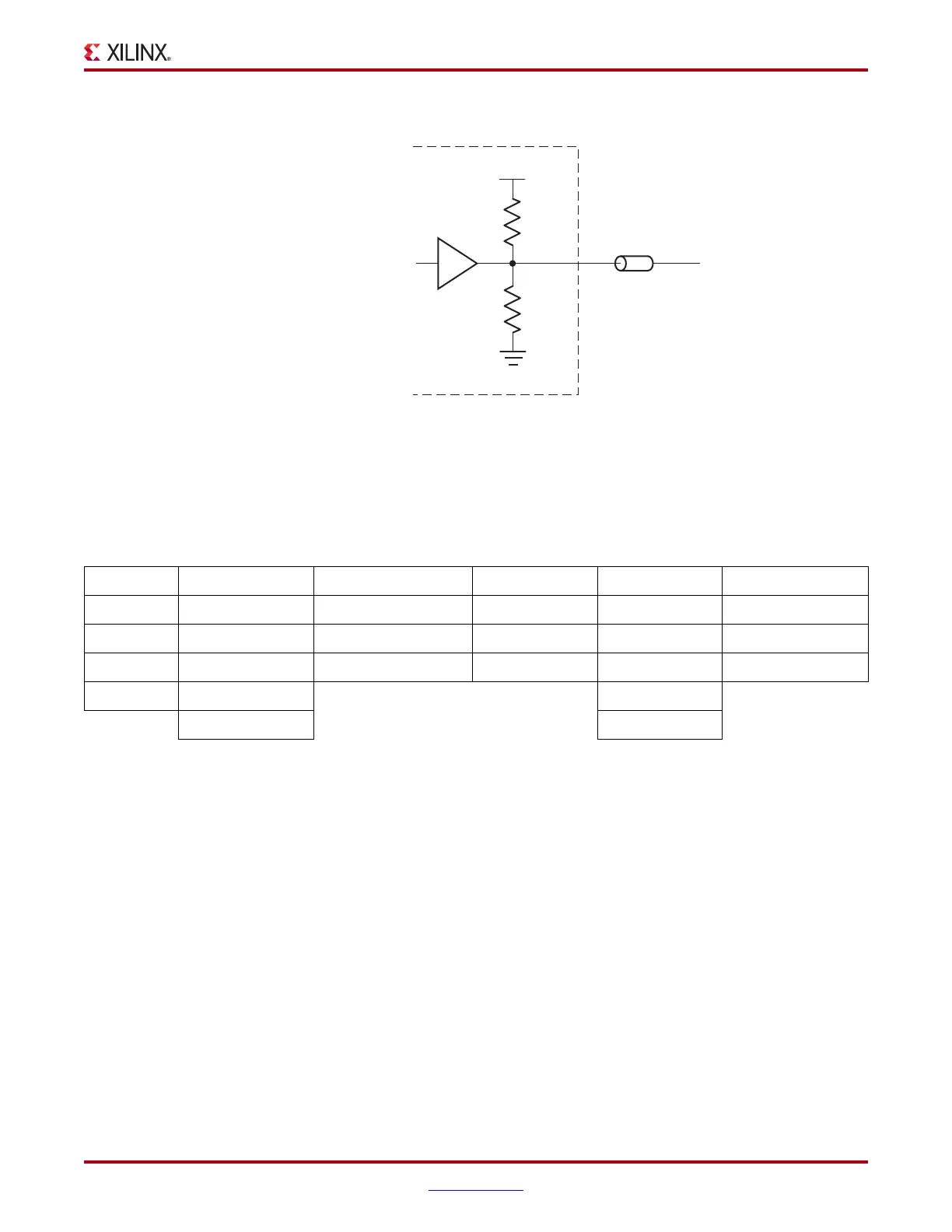
Figure 6-15 illustrates a driver with split termination inside a Virtex-5 device.
DCI in Virtex-5 Device I/O Standards
DCI works with single-ended I/O standards. DCI supports the standards shown in
Table 6-3.
To correctly use DCI in a Virtex-5 device, users must follow the following rules:
1. V
CCO
pins must be connected to the appropriate V
CCO
voltage based on the
IOSTANDARDs in that bank.
2. Correct DCI I/O buffers must be used in the software either by using IOSTANDARD
attributes or instantiations in the HDL code.
3. Some DCI standards require connecting the external reference resistors to the
multipurpose pins (VRN and VRP) in the bank. Where this is required, these two
multipurpose pins cannot be used as general-purpose I/O. Refer to the Virtex-5 FPGA
pinout tables for the specific pin locations. Pin VRN must be pulled up to V
CCO
by its
reference resistor. Pin VRP must be pulled down to ground by its reference resistor.
Some DCI standards do not require connecting the external reference resistors to the
VRP/VRN pins. When these DCI-based I/O standards are the only ones in a bank, the
the VRP and VRN pins in that bank can be used as general-purpose I/O.
X-Ref Target - Figure 6-15
Figure 6-15: Driver with Termination to V
CCO
/2 Using DCI Split Termination
2R
2R
UG190_6_13_021206
V
CCO
IOB
Z
0
Virtex-5 DCI
Table 6-3: Virtex-5 Device DCI I/O Standards
LVDCI HSTL_I_DCI DIFF_HSTL_I_DCI HSTL_III_DCI SSTL2_I_DCI DIFF_SSTL2_I_DCI
HSLVDCI HSTL_I_DCI_18 DIFF_HSTL_I_DCI_18
HSTL_III_DCI_18
SSTL2_II_DCI DIFF_SSTL2_II_DCI
LVDCI_DV2 HSTL_II_DCI DIFF_HSTL_II_DCI HSTL_IV_DCI SSTL18_I_DCI DIFF_SSTL18_I_DCI
GTL_DCI HSTL_II_DCI_18
DIFF_HSTL_II_DCI_18 HSTL_IV_DCI_18
SSTL18_II_DCI
DIFF_SSTL18_II_DCI
GTLP_DCI HSTL_II_T_DCI SSTL2_II_T_DCI
HSTL_II_T_DCI_18 SSTL18_II_T_DCI
 Loading...


