252 www.xilinx.com Virtex-5 FPGA User Guide
UG190 (v5.0) June 19, 2009
Chapter 6: SelectIO Resources
HSTL Class I
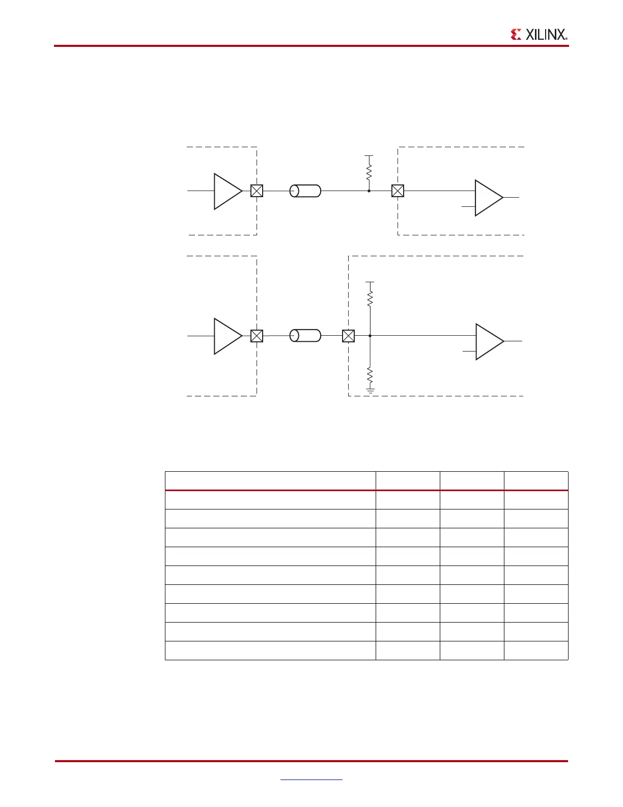
Figure 6-40 shows a sample circuit illustrating a valid termination technique for HSTL
Class I.
Table 6-15 lists the HSTL Class I DC voltage specifications.
X-Ref Target - Figure 6-40
Figure 6-40: HSTL Class I Termination
Table 6-15: HSTL Class I DC Voltage Specifications
Min Typ Max
V
CCO
1.40 1.50 1.60
V
REF
(2)
0.68 0.75 0.90
V
TT
– V
CCO
× 0.5 –
V
IH
V
REF
+0.1 – –
V
IL
––V
REF
–0.1
V
OH
V
CCO
–0.4 – –
V
OL
– – 0.4
I
OH
at V
OH
(mA)
(1)
–8 – –
I
OL
at V
OL
(mA)
(1)
8 – –
Notes:
1. V
OL
and V
OH
for lower drive currents are sample tested.
2. Per EIA/JESD8-6, “The value of V
REF
is to be selected by the user to provide optimum noise margin in
the use conditions specified by the user.”
Z
0
IOB
IOB
HSTL_I
HSTL_I
ug190_6_38_030206
V
TT
= 0.75V
R
P
= Z
0
= 50Ω
Z
0
IOB
IOB
HSTL_I_DCI HSTL_I_DCI
V
CCO
= 1.5V
2R
VRP
= 2Z
0
= 100Ω
2R
VRN
= 2Z
0
= 100Ω
V
REF
= 0.75V
+
–
V
REF
= 0.75V
+
–
External Termination
DCI
 Loading...


