206 www.xilinx.com Virtex-5 FPGA User Guide
UG190 (v5.0) June 19, 2009
Chapter 5: Configurable Logic Blocks (CLBs)
Distributed RAM Timing Characteristics
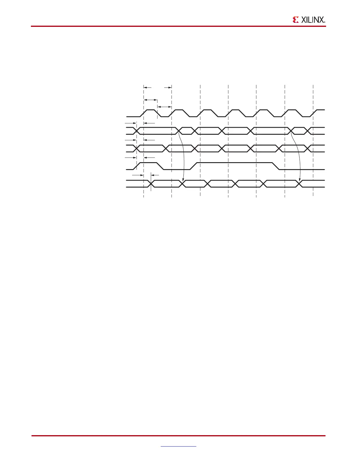
The timing characteristics of a 16-bit distributed RAM implemented in a Virtex-5 FPGA
slice (LUT configured as RAM) are shown in Figure 5-28.
Clock Event 1: Write Operation
During a Write operation, the contents of the memory at the address on the ADDR inputs
are changed. The data written to this memory location is reflected on the A/B/C/D
outputs synchronously.
• At time T
WS
before clock event 1, the write-enable signal (WE) becomes valid-High,
enabling the RAM for a Write operation.
• At time T
AS
before clock event 1, the address (2) becomes valid at the A/B/C/D
inputs of the RAM.
• At time T
DS
before clock event 1, the DATA becomes valid (1) at the DI input of the
RAM and is reflected on the A/B/C/D output at time T
SHCKO
after clock event 1.
This is also applicable to the AMUX, BMUX, CMUX, DMUX, and COUT outputs at time
T
SHCKO
and T
WOSCO
after clock event 1.
Clock Event 2: Read Operation
All Read operations are asynchronous in distributed RAM. As long as WE is Low, the
address bus can be asserted at any time. The contents of the RAM on the address bus are
reflected on the A/B/C/D outputs after a delay of length T
ILO
(propagation delay through
a LUT). The address (F) is asserted after clock event 2, and the contents of the RAM at
address (F) are reflected at the output after a delay of length T
ILO
.
X-Ref Target - Figure 5-28
Figure 5-28: Slice Distributed RAM Timing Characteristics
UG190_5_28_050506
T
WPL
T
WPH
T
WC
1234567
CLK
WE
DATA_OUT
A/B/C/D
Output
A/B/C/D
(ADDR)
AX/BX/CX/DX
(DI)
T
AS
2
1
10 01MEM(F)
WRITE WRITE WRITE WRITEREAD READ
MEM(E)
XX001
F3 4 5 E
T
DS
T
WS
T
ILO
T
ILO
T
SHCKO
 Loading...


