138 www.xilinx.com Virtex-5 FPGA User Guide
UG190 (v5.0) June 19, 2009
Chapter 4: Block RAM
Block RAM Timing Model
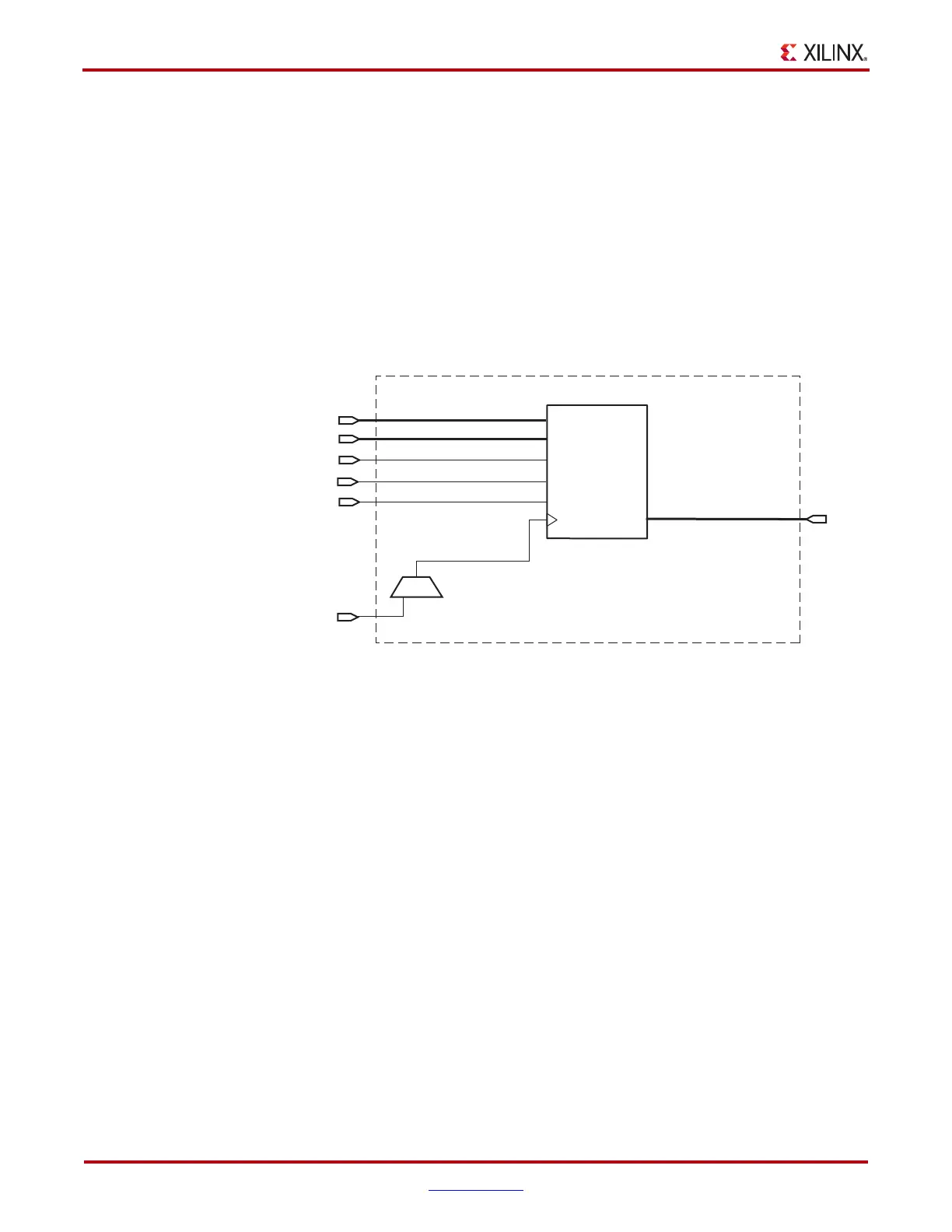
Figure 4-15 illustrates the delay paths associated with the implementation of block RAM.
This example takes the simplest paths on and off chip (these paths can vary greatly
depending on the design). This timing model demonstrates how and where the block
RAM timing parameters are used.
• NET = Varying interconnect delays
• T
IOPI
= Pad to I-output of IOB delay
• T
IOOP
= O-input of IOB to pad delay
• T
BCCKO_O
= BUFGCTRL delay
X-Ref Target - Figure 4-15
Figure 4-15: Block RAM Timing Model
Block RAM
ug190_4_14_022207
FPGA
[T
IOPI
+ NET] + T
RCCK_WEN
Write Enable
[T
IOPI
+ NET] + T
RCCK_EN
Enable
[T
IOPI
+ NET] + T
RCCK_ADDR
Address
[T
IOPI
+ NET] + T
RDCK_DI
Data
[T
BCCKO_O
+ NET]
Clock
[T
IOPI
+ NET]
BUFGCTRL
T
RCKO_DO
+ [NET + T
IOOP
]
Data
[T
IOPI
+ NET] + T
RCCK_SSR
Synchronous
Set/Reset
DO
DI
ADDR
WE
EN
SSR
CLK
 Loading...


