Virtex-5 FPGA User Guide www.xilinx.com 277
UG190 (v5.0) June 19, 2009
Specific Guidelines for I/O Supported Standards
Table 6-28 lists the SSTL2 DC voltage specifications for Class I.
Differential SSTL2 Class I (2.5V)
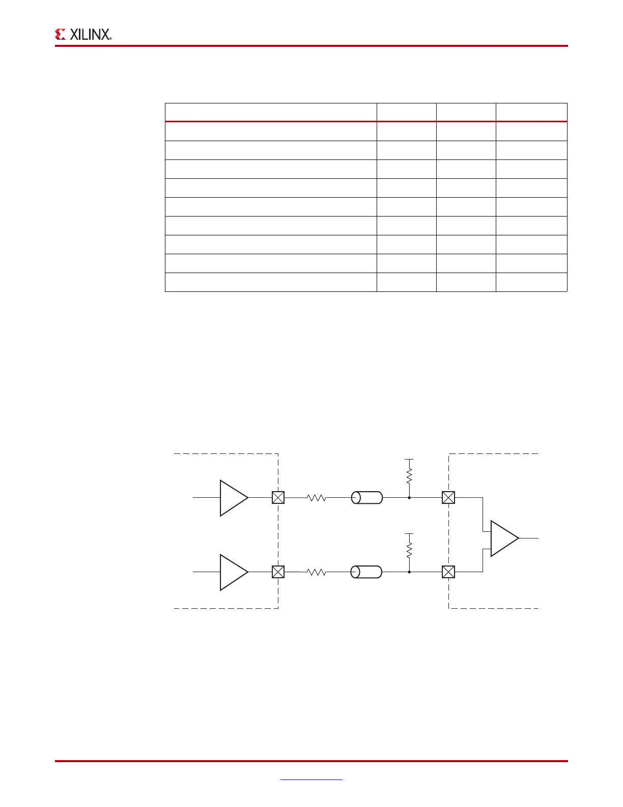
Figure 6-68 shows a sample circuit illustrating a valid termination technique for
differential SSTL2 Class I (2.5V) with unidirectional termination.
Table 6-28: SSTL2 DC Voltage Specifications Class I
Min Typ Max
V
CCO
2.3 2.5 2.7
V
REF
=0.5× V
CCO
1.13 1.25 1.38
V
TT
=V
REF
+N
(1)
1.09 1.25 1.42
V
IH
≥ V
REF
+ 0.15 1.28 1.4 V
CCO
+0.3
(2)
V
IL
≤ V
REF
– 0.15 –0.3
(3)
1.1 1.23
V
OH
≥ V
REF
+ 0.61 1.74 1.84 1.94
V
OL
≤ V
REF
–0.61
(4)
0.56 0.66 0.76
I
OH
at V
OH
(mA) –8.1 – –
I
OL
at V
OL
(mA) 8.1 – –
Notes:
1. N must be greater than or equal to –0.04 and less than or equal to 0.04.
2. V
IH
maximum is V
CCO
+0.3.
3. V
IL
minimum does not conform to the formula.
4. Because SSTL2_I_DCI uses a controlled-impedance driver, V
OH
and V
OL
are different.
X-Ref Target - Figure 6-68
Figure 6-68: Differential SSTL2 Class I Unidirectional Termination
ug190_6_64_030506
+
–
External Termination
Z
0
IOB
IOB
DIFF_SSTL2_I
DIFF_SSTL2_I
Z
0
DIFF_SSTL2_I
V
TT
= 1.25V
V
TT
= 1.25V
R
P
= Z
0
= 50Ω
50Ω
R
S
= 25Ω
R
S
= 25Ω
 Loading...


