274 www.xilinx.com Virtex-5 FPGA User Guide
UG190 (v5.0) June 19, 2009
Chapter 6: SelectIO Resources
HSTL Class I (1.2V)
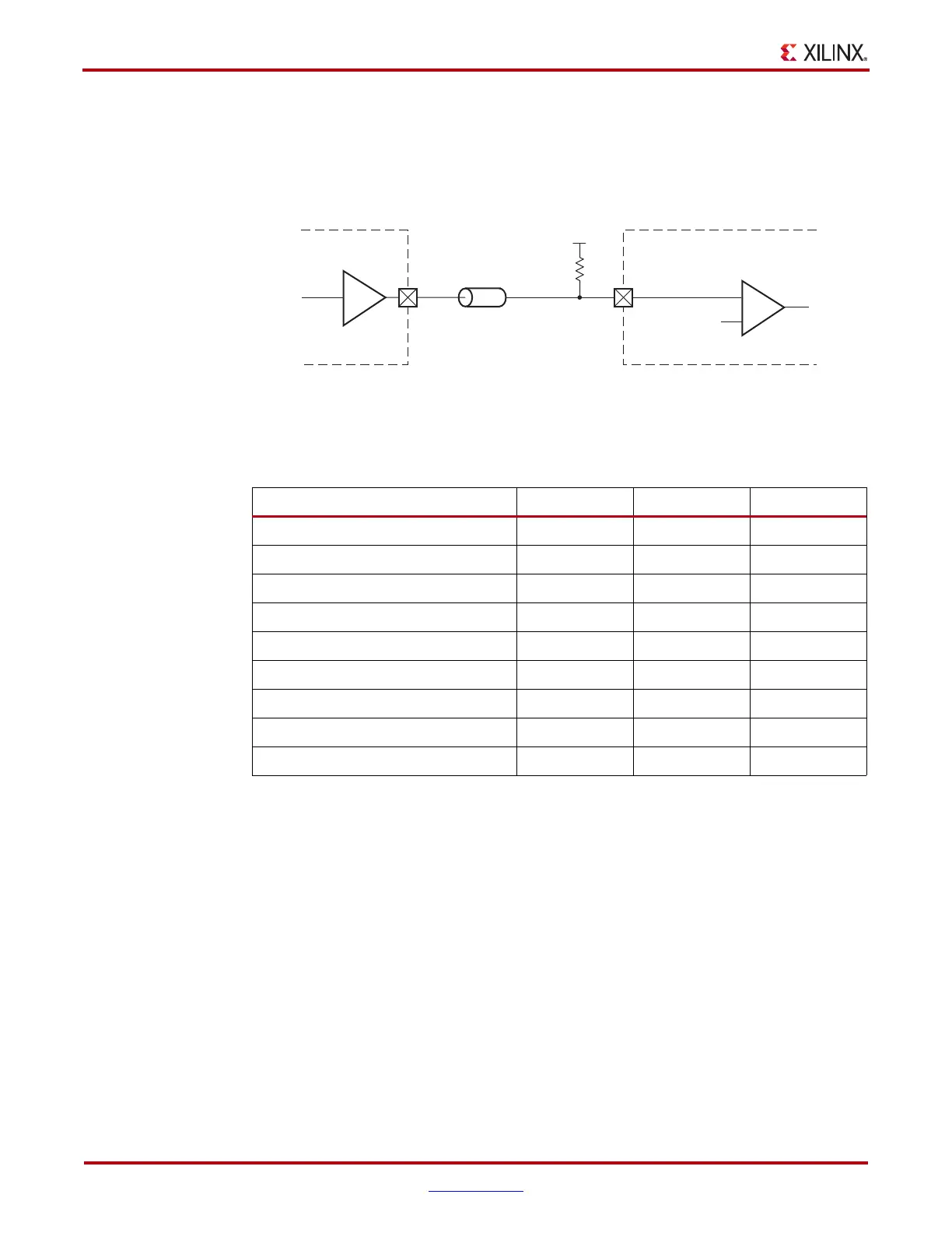
Figure 6-66 shows a sample circuit illustrating a valid termination technique for HSTL
Class I (1.2V). It is used for unidirectional links.
Table 6-21 lists the HSTL Class I (1.2V) DC voltage specifications.
SSTL (Stub-Series Terminated Logic)
The Stub-Series Terminated Logic (SSTL) for 2.5V (SSTL2) and 1.8V (SSTL18) standards are
for general purpose memory buses. SSTL2 is defined by the JEDEC standard JESD8-9B and
SSTL18 is defined by the JEDEC standard JESD8-15. The SSTL2 standard has two classes;
Class I is for unidirectional and class II is for bidirectional signaling. Virtex-5 FPGA I/O
supports both standards for single-ended signaling and differential signaling. This
standard requires a differential amplifier input buffer and a push-pull output buffer.
X-Ref Target - Figure 6-66
Figure 6-66: HSTL Class I (1.2V) Termination
Table 6-27: HSTL Class I (1.2V) DC Voltage Specifications
Min Typ Max
V
CCO
1.14 1.2 1.26
V
REF
(2)
V
CCO
× 0.48 0.6 V
CCO
× 0.52
V
TT
– V
CCO
× 0.5 –
V
IH
V
REF
+0.08 – –
V
IL
––V
REF
–0.08
V
OH
V
CCO
– .0.315 – –
V
OL
– – 0.315
I
OH
at V
OH
(mA)
(1)
–6.3 – –
I
OL
at V
OL
(mA)
(1)
6.3 – –
Notes:
1. V
OL
and V
OH
for lower drive currents are sample tested.
2. Per EIA/JESD8-6, “The value of V
REF
is to be selected by the user to provide optimum noise margin in
the use conditions specified by the user.”
Z
0
IOB
IOB
HSTL_I_12
HSTL_I_12
ug190_6_62_030306
V
TT
= 0.6V
R
P
= Z
0
= 50Ω
V
REF
= 0.6V
+
–
External Termination
 Loading...


