Virtex-5 FPGA User Guide www.xilinx.com 87
UG190 (v5.0) June 19, 2009
DCM Timing Models
Status Flags
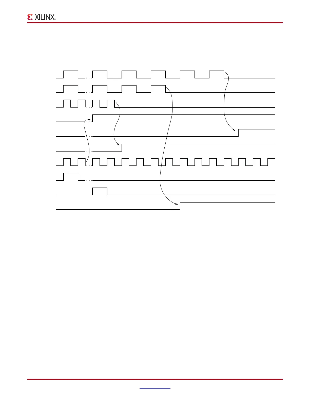
The example in Figure 2-20 shows the behavior of the status flags in the event of a phase-
shift overflow and CLKIN/CLKFB/CLKFX failure.
• Clock Event 1
Prior to the beginning of this timing diagram, CLK0 (not shown) is already phase-
shifted at its maximum value. At clock event 1, PSDONE is asserted. However, since
the DCM has reached its maximum phase-shift capability no phase adjustment is
performed. Instead, the phase-shift overflow status pin DO(0) is asserted to indicate
this condition.
• Clock Event 2
The CLKFX output stops toggling. Within 257 to 260 clock cycles after this event, the
CLKFX stopped status DO(2) is asserted to indicate that the CLKFX output stops
toggling.
• Clock Event 3
The CLKFB input stops toggling. Within 257 to 260 clock cycles after this event, the
CLKFB stopped status DO(3) is asserted to indicate that the CLKFB output stops
toggling.
• Clock Event 4
The CLKIN input stops toggling. Within 9 clock cycles after this event, DO(1) is
asserted to indicate that the CLKIN output stops toggling.
X-Ref Target - Figure 2-20
Figure 2-20: Status Flags Example
CLKIN
3
4
2
257 - 260 Cycles
CLKFB
PSEN
PSDONE
CLKFX
DO(0)
1
PSCLK
ug190_2_21_042406
DO(1)
DO(2)
DO(3)
 Loading...


