Virtex-5 FPGA User Guide www.xilinx.com 377
UG190 (v5.0) June 19, 2009
Output Parallel-to-Serial Logic Resources (OSERDES)
OSERDES Latencies
The input to output latencies of OSERDES blocks depend on the DATA_RATE and
DATA_WIDTH attributes. Latency is defined as a period of time between the following
two events: (a) when the rising edge of CLKDIV clocks the data at inputs D1–D6 into the
OSERDES, and (b) when the first bit of the serial stream appears at OQ. Table 8-10
summarizes the various OSERDES latency values.
OSERDES Timing Model and Parameters
This section discusses all timing models associated with the OSERDES primitive.
Table 8-11 describes the function and control signals of the OSERDES switching
characteristics in the Virtex-5 FPGA Data Sheet.
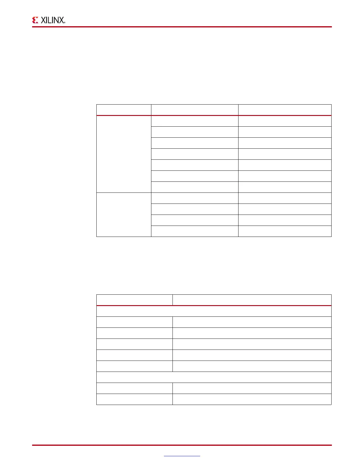
Table 8-10: OSERDES Latencies
DATA_RATE DATA_WIDTH Latency
SDR
2:1 1 CLK cycle
3:1 3 CLK cycles
4:1 4 CLK cycles
5:1 4 CLK cycles
6:1 5 CLK cycles
7:1 5 CLK cycles
8:1 6 CLK cycles
DDR
4:1 1 CLK cycle
6:1 3 CLK cycles
8:1 4 CLK cycles
10:1 4 CLK cycles
Table 8-11: OSERDES Switching Characteristics
Symbol Description
Setup/Hold
T
OSDCK_D
/T
OSCKD_D
D input Setup/Hold with respect to CLKDIV
T
OSDCK_T
/T
OSCKD_T
T input Setup/Hold with respect to CLK
T
OSDCK_T
/T
OSCKD_T
T input Setup/Hold with respect to CLKDIV
T
OSCCK_OCE
/T
OSCKC_OCE
OCE input Setup/Hold with respect to CLK
T
OSCCK_TCE
/T
OSCKC_TCE
TCE input Setup/Hold with respect to CLK
Sequential Delays
T
OSCKO_OQ
Clock to Out from CLK to OQ
T
OSCKO_TQ
Clock to Out from CLK to TQ
 Loading...


