122 www.xilinx.com Virtex-5 FPGA User Guide
UG190 (v5.0) June 19, 2009
Chapter 4: Block RAM
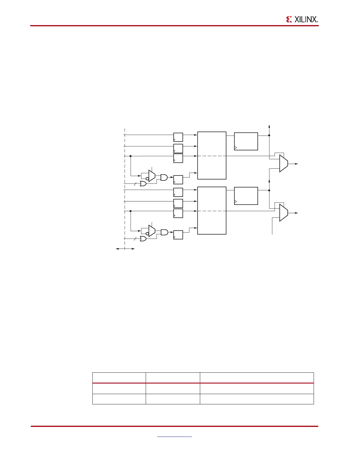
Cascadable Block RAM
In the Virtex-5 block RAM architecture, two 32K x 1 RAMs can be combined to form one
64K x 1 RAM without using local interconnect or additional CLB logic resources. Any two
adjacent block RAMs can be cascaded to generate a 64K x 1 block RAM. Increasing the
depth of the block RAM by cascading two block RAMs is available only in the 64K x 1
mode. Further information on cascadable block RAM is described in the “Additional
RAMB18 and RAMB36 Primitive Design Considerations” section. For other wider and/or
deeper sizes, consult the Creating Larger RAM Structures section. Figure 4-7 shows the
block RAM with the appropriate ports connected in the Cascadable mode.
Byte-wide Write Enable
The byte-wide write enable feature of the block RAM gives the capability to write eight bit
(one byte) portions of incoming data. There are four independent byte-wide write enable
inputs to the RAMB36 true dual-port RAM. There are eight independent byte-wide write
enable inputs to block RAM in simple dual-port mode (RAMB36SDP). Table 4-4
summarizes the byte-wide write enables for the 36K and 18K block RAM. Each byte-wide
write enable is associated with one byte of input data and one parity bit. All byte-wide
write enable inputs must be driven in all data width configurations. This feature is useful
when using block RAM to interface with a microprocessor. Byte-wide write enable is not
available in the multirate FIFO or ECC mode. Byte-wide write enable is further described
in the “Additional RAMB18 and RAMB36 Primitive Design Considerations” section.
Figure 4-8 shows the byte-wide write-enable timing diagram for the RAMB36.
X-Ref Target - Figure 4-7
Figure 4-7: Cascadable Block RAM
D0
Not Used
DI
DI
CASCADEIN
Connect to logic High or Low
CASCADEOUT
(No Connect)
A[14:0]
WE
D0
A15
A15
A[14:0]
D0
DI
DI
A[14:0]
WE
D0
DQ
DQ
DQ
DQ
DQ
DQ
DQ
DQ
A15
A15
A[14:0]
WE[3:0]
WE[3:0]
Interconnect
Block RAM
RAM_EXTENSION =
UPPER(0)
RAM_EXTENSION =
LOWER(1)
0
1
0
1
0
1
0
1
ug190_4_07_071607
CASCADEIN of Top
CASCADEOUT of Bottom
Optional
Output FF
Optional
Output FF
Table 4-4: Available Byte-wide Write Enables
Primitive Maximum Bit Width Number of Byte-wide Write Enables
RAMB36 36 4
RAMB36SDP 72 8
 Loading...


