244 www.xilinx.com Virtex-5 FPGA User Guide
UG190 (v5.0) June 19, 2009
Chapter 6: SelectIO Resources
LVD CI _DV2
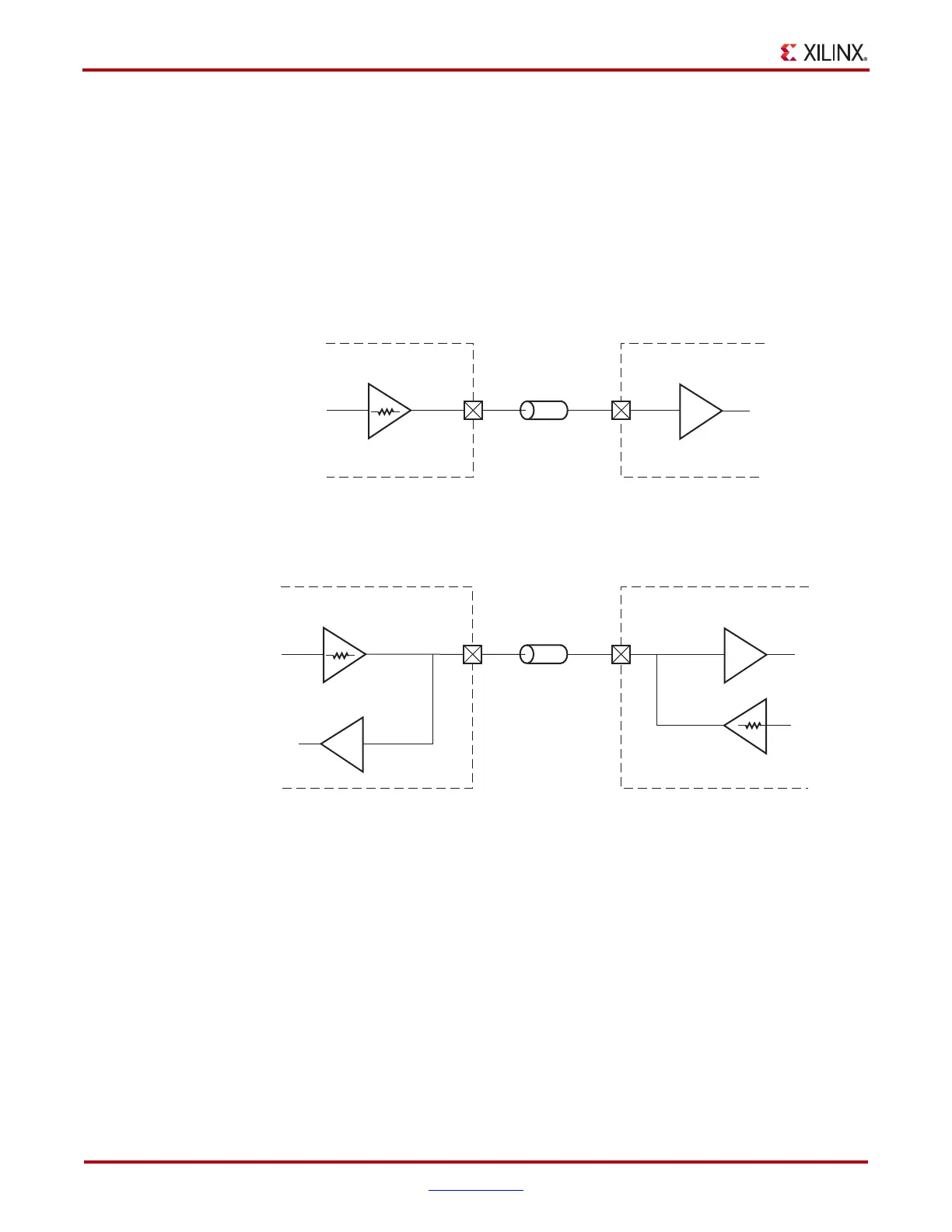
A controlled impedance driver with half impedance (source termination) can also provide
drivers with one half of the impedance of the reference resistors. This allows reference
resistors to be twice as large, thus reducing static power consumption through VRN/VRP.
The I/O standards supporting a controlled impedance driver with half impedance are:
LVDCI_DV2_15, LVDCI_DV2_18, and LVDCI_DV2_25. Figure 6-33 and Figure 6-34
illustrate a controlled driver with half impedance unidirectional and bidirectional
termination.
To match the drive impedance to Z
0
when using a driver with half impedance, the
reference resistor R must be twice Z
0
.
There are no drive strength settings for LVDCI drivers. When the driver impedance is one-
half of the VRN/VRP reference resistors, it is indicated by the addition of DV2 to the
attribute name.
Table 6-9 lists the LVCMOS, LVDCI, and LVDCI_DV2 voltage specifications.
X-Ref Target - Figure 6-33
Figure 6-33: Controlled Impedance Driver with Half Impedance
Unidirectional Termination
X-Ref Target - Figure 6-34
Figure 6-34: Controlled Impedance Driver with Half Impedance
Bidirectional Termination
Z
0
IOB
IOB
LVDCI_DV2
LVDCI_DV2
ug190_6_30_022806
R
0
= ½R
VRN
= ½R
VRP
= Z
0
Z
0
IOB
IOB
LVDCI_DV2
LVDCI_DV2
ug190_6_31_022806
R
0
= ½R
VRN
= ½R
VRP
= Z
0
R
0
= ½R
VRN
= ½R
VRP
= Z
0
 Loading...


