Virtex-5 FPGA User Guide www.xilinx.com 135
UG190 (v5.0) June 19, 2009
Block RAM Timing Model
Block RAM Timing Parameters
Table 4-11 shows the Virtex-5 FPGA block RAM timing parameters.
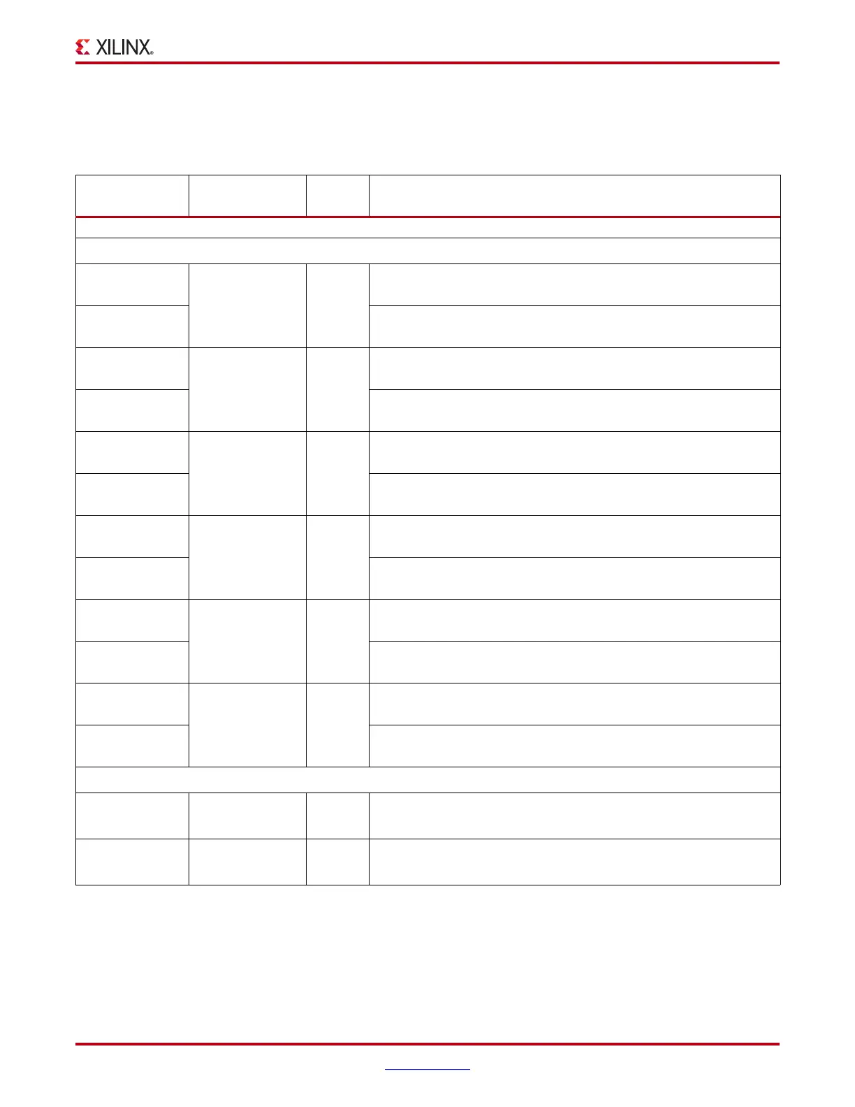
Table 4-11: Block RAM Timing Parameters
Parameter Function
Control
Signal
Description
Setup and Hold Relative to Clock (CLK)
T
RxCK_x
= Setup time (before clock edge) and T
RCKx_x
= Hold time (after clock edge)
T
RCCK_ADDR
Address inputs ADDR
Time before the clock that address signals must be stable at the
ADDR inputs of the block RAM.
(1)
T
RCKC_ADDR
Time after the clock that address signals must be stable at the ADDR
inputs of the block RAM.
(1)
T
RDCK_DI
Data inputs DI
Time before the clock that data must be stable at the DI inputs of the
block RAM.
T
RCKD_DI
Time after the clock that data must be stable at the DI inputs of the
block RAM.
T
RCCK_EN
Enable EN
Time before the clock that the enable signal must be stable at the EN
input of the block RAM.
T
RCKC_EN
Time after the clock that the enable signal must be stable at the EN
input of the block RAM.
T
RCCK_SSR
Synchronous
Set/Reset
SSR
Time before the clock that the synchronous set/reset signal must be
stable at the SSR input of the block RAM.
T
RCKC_SSR
Time after the clock that the synchronous set/reset signal must be
stable at the SSR input of the block RAM.
T
RCCK_WE
Write Enable WE
Time before the clock that the write enable signal must be stable at
the WE input of the block RAM.
T
RCKC_WE
Time after the clock that the write enable signal must be stable at the
WE input of the block RAM.
T
RCCK_REGCE
Optional Output
Register Enable
REGCE
Time before the CLK that the register enable signal must be stable at
the REGCE input of the block RAM.
T
RCKC_REGCE
Time after the clock that the register enable signal must be stable at
the REGCE input of the block RAM.
Clock to Out Delays
T
RCKO_DO
(latch mode)
Clock to Output CLK to
DO
Time after the clock that the output data is stable at the DO outputs
of the block RAM (without output register).
T
RCKO_DO
(register mode)
Clock to Output CLK to
DO
Time after the clock that the output data is stable at the DO outputs
of the block RAM (with output register).
Notes:
1. While EN is active, ADDR inputs must be stable during the entire setup/hold time window, even if WE is inactive. Violating this
requirement can result in block RAM data corruption. If ADDR timing could violate the specified requirements, EN must be inactive
(disabled).
 Loading...


