Virtex-5 FPGA User Guide www.xilinx.com 211
UG190 (v5.0) June 19, 2009
CLB Primitives
• At time T
CINCK
before clock event 1, data from CIN input becomes valid-High at the
D input of the slice register. This is reflected on any of the AQ/BQ/CQ/DQ pins at
time T
CKO
after clock event 1.
• At time T
SRCK
before clock event 3, the SR signal (configured as synchronous reset)
becomes valid-High, resetting the slice register. This is reflected on any of the
AQ/BQ/CQ/DQ pins at time T
CKO
after clock event 3.
CLB Primitives
More information on the CLB primitives are available in the software libraries guide.
Distributed RAM Primitives
Seven primitives are available; from 32 x 2 bits to 256 x 1 bit. Three primitives are single-
port RAM, two primitives are dual-port RAM, and two primitives are quad-port RAM, as
shown in Table 5-11.
The input and output data are 1-bit wide (with the exception of the 32-bit RAM).
Figure 5-32 shows generic single-port, dual-port, and quad-port distributed RAM
primitives. The A, ADDR, and DPRA signals are address buses.
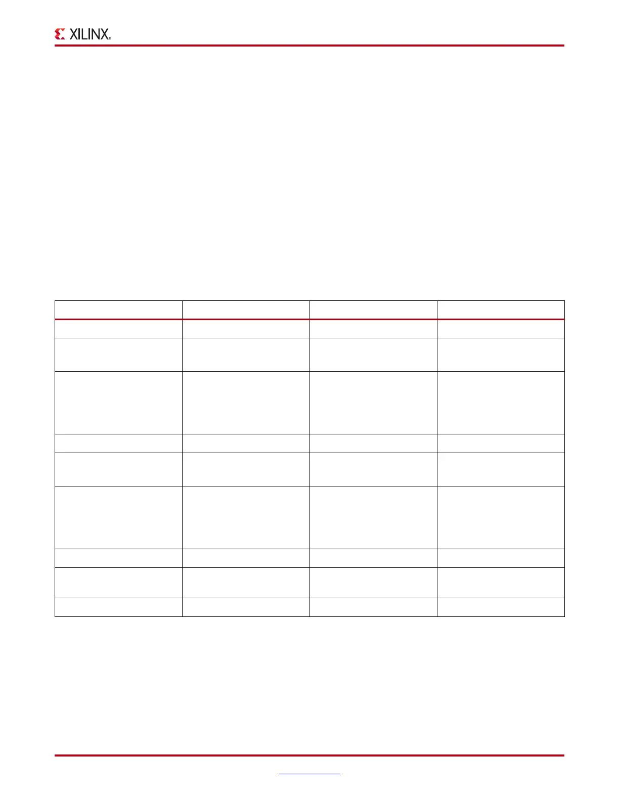
Table 5-11: Single-Port, Dual-Port, and Quad-Port Distributed RAM
Primitive RAM Size Type Address Inputs
RAM32X1S 32-bit Single-port A[4:0] (read/write)
RAM32X1D 32-bit Dual-port A[4:0] (read/write)
DPRA[4:0] (read)
RAM32M 32-bit Quad-port ADDRA[4:0] (read)
ADDRB[4:0] (read)
ADDRC[4:0] (read)
ADDRD[4:0] (read/write)
RAM64X1S 64-bit Single-port A[5:0] (read/write)
RAM64X1D 64-bit Dual-port A[5:0] (read/write)
DPRA[5:0] (read)
RAM64M 64-bit Quad-port ADDRA[5:0] (read)
ADDRB[5:0] (read)
ADDRC[5:0] (read)
ADDRD[5:0] (read/write)
RAM128X1S 128-bit Single-port A[6:0] (read/write)
RAM128X1D 128-bit Dual-port A[6:0], (read/write)
DPRA[6:0] (read)
RAM256X1S 256-bit Single-port A[7:0] (read/write)
 Loading...


