284 www.xilinx.com Virtex-5 FPGA User Guide
UG190 (v5.0) June 19, 2009
Chapter 6: SelectIO Resources
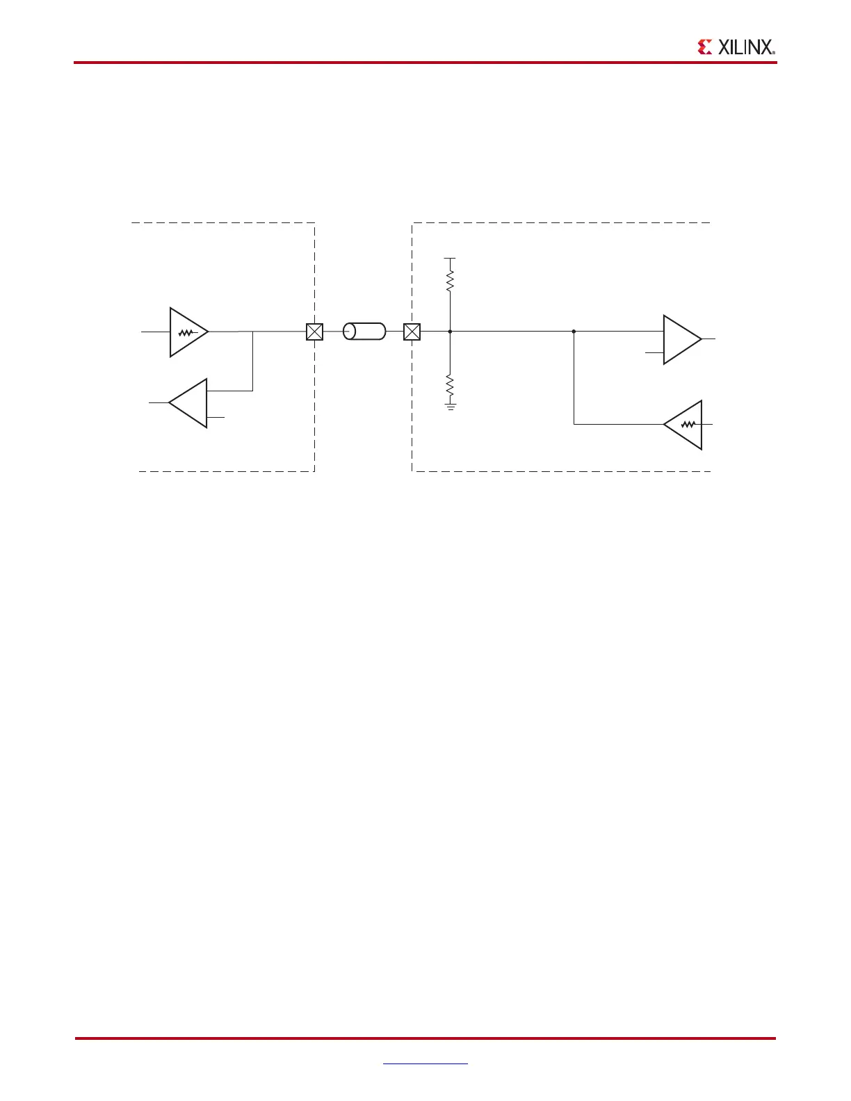
SSTL2_II_T_DCI (2.5V) Split-Thevenin Termination
Figure 6-76 shows a sample circuit illustrating a valid termination technique for
SSTL2_II_T_DCI (2.5V) with on-chip split-Thevenin termination. In this bidirectional I/O
standard, when 3-stated, the termination is invoked on the receiver and not on the driver.
X-Ref Target - Figure 6-76
Figure 6-76: SSTL2_II_T_DCI (2.5V) Split-Thevenin Termination
ug190_6_92_041206
Z
0
IOB
IOB
SSTL2_II_T_DCI
SSTL2_II_T_DCI
V
CCO
= 2.5V
2R
VRP
= 2Z
0
= 100Ω
2R
VRN
= 2Z
0
= 100Ω
V
REF
= 1.25V
+
–
DCI
R
0
= 25Ω
V
REF
= 1.25V
R
0
= 25Ω
Not 3-stated 3-stated
 Loading...


