208 www.xilinx.com Virtex-5 FPGA User Guide
UG190 (v5.0) June 19, 2009
Chapter 5: Configurable Logic Blocks (CLBs)
Slice SRL Timing Parameters
Table 5-9 shows the SLICEM SRL timing parameters for a majority of the paths in
Figure 5-29.
Slice SRL Timing Characteristics
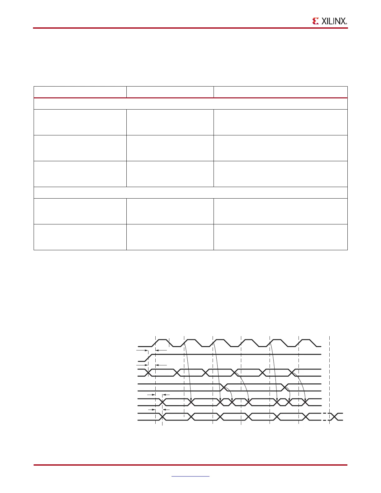
Figure 5-30 illustrates the timing characteristics of a 16-bit shift register implemented in a
Virtex-5 FPGA slice (a LUT configured as an SRL).
Table 5-9: Slice SRL Timing Parameters
Parameter Function Description
Sequential Delays for a Slice LUT Configured as an SRL
T
REG
(1)
CLK to A/B/C/D outputs Time after the CLK of a write operation that the
data written to the SRL is stable on the A/B/C/D
outputs of the slice.
T
REG_MUX
(1)
CLK to AMUX - DMUX output Time after the CLK of a write operation that the
data written to the SRL is stable on the DMUX
output of the slice.
T
REG_M31
CLK to DMUX output via
MC31 output
Time after the CLK of a write operation that the
data written to the SRL is stable on the DMUX
output via MC31 output.
Setup and Hold Times for a Slice LUT Configured SRL
(2)
T
WS
/T
WH
CE input (WE) Time before/after the clock that the write enable
signal must be stable at the WE input of the slice
LUT (configured as an SRL).
T
DS
/T
DH
(3)
AX/BX/CX/DX configured as
data input (DI)
Time before the clock that the data must be stable
at the AX/BX/CX/DX input of the slice
(configured as an SRL).
Notes:
1. This parameter includes a LUT configured as a two-bit shift register.
2. T
XXCK
= Setup Time (before clock edge), and T
CKXX
= Hold Time (after clock edge).
3. Parameter includes AI/BI/CI/DI configured as a data input (DI2) or two bits with a common shift.
X-Ref Target - Figure 5-30
Figure 5-30: Slice SRL Timing Characteristics
ug190_5_30_050506
123456 32
CLK
Write Enable
(WE)
Shift_In (DI)
Address
(A/B/C/D)
Data Out
(A/B/C/D)
MSB
(MC31/DMUX)
T
DS
T
ILO
T
ILO
0110 1 0
20
X
XXXXXXX0
011 11 100
T
REG
T
REG
T
WS
1
 Loading...


