Virtex-5 FPGA User Guide www.xilinx.com 337
UG190 (v5.0) June 19, 2009
Input/Output Delay Element (IODELAY)
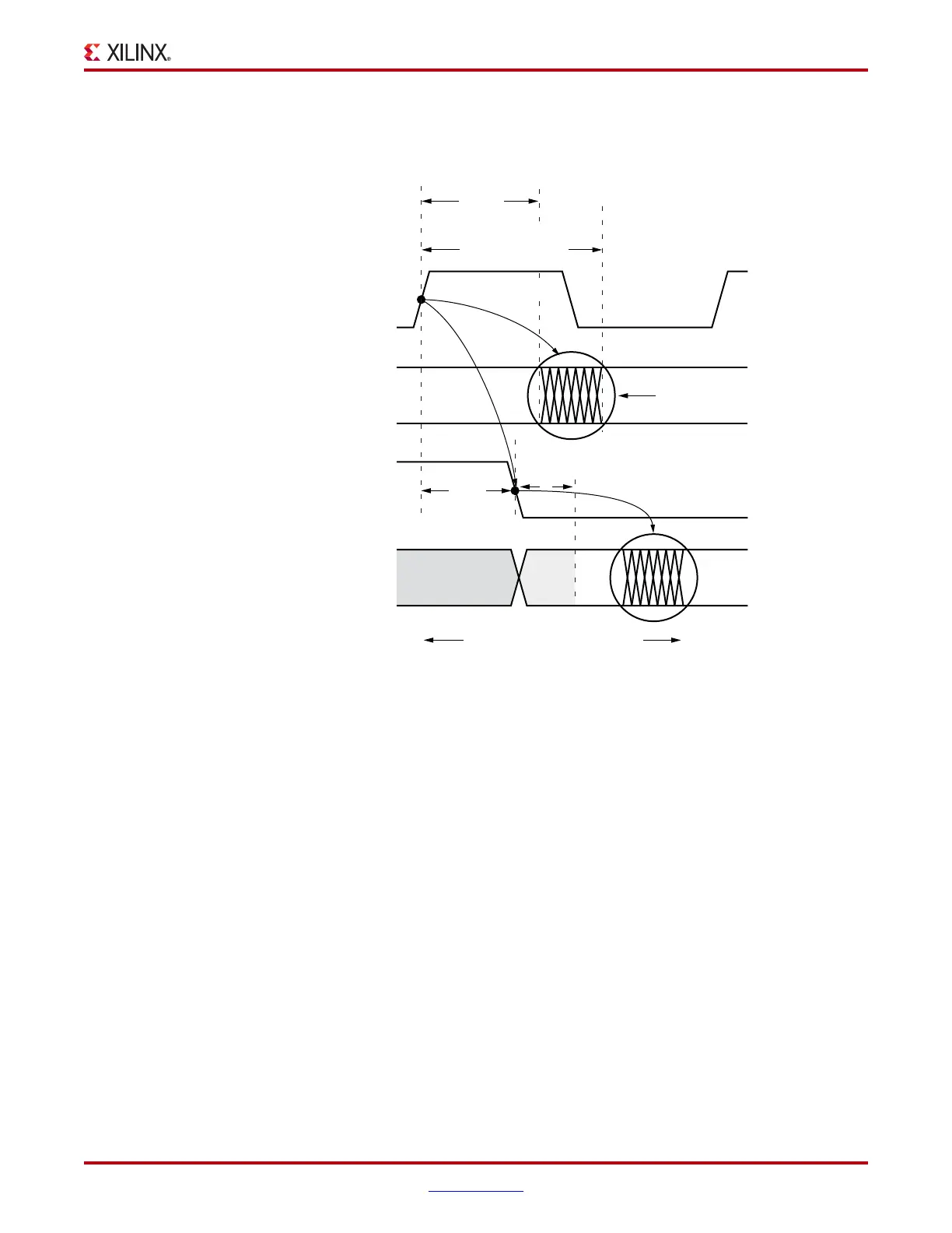
The timing diagram in Figure 7-14 shows the relevant signal timing for the case where the
I/O switches from input to an output using 3-state control. The switching characteristics
shown in the diagram are specified in the Virtex-5 FPGA Data Sheet.
3-state control activities on the OBUF of the IOB and ODDR flip-flop to PAD timing are in
parallel with each other, depending on the ODELAY_VALUE setting the final output value
in response to a clock edge at the ODDR CLK pin is valid before or after the pad is driven
from the 3-state control. After the 3-state control propagates through to the PAD and the
IODELAY is turned around, the clock-to-output time of the ODDR flip-flop through the
IODELAY element (with the ODELAY_VALUE setting) solely determines the clock-to-
output time to the pad.
IDELAYCTRL Overview
If the IODELAY or ISERDES primitive is instantiated with the IOBDELAY_TYPE attribute
set to FIXED or VARIABLE, the IDELAYCTRL module must be instantiated. The
IDELAYCTRL module continuously calibrates the individual delay elements (IODELAY)
in its region (see Figure 7-17, page 340), to reduce the effects of process, voltage, and
temperature variations. The IDELAYCTRL module calibrates IODELAY using the user
supplied REFCLK.
X-Ref Target - Figure 7-14
Figure 7-14: Relevant Timing Signals used to Examine IODELAY Timing when an
IOB Changes from an Input to an Output
IODELAY_05_082107
ODDR CLK
DATAO U T
Previous PAD
input value
TSCONTROL
PA D
Clock to DATAOUT is variable
based on internal timing the
ODELAY_VALUE (0-63)
Clock-to-Out with
ODELAY_VALUE = 0
Clock to PAD being driven or
T
OCKQ
+ T
IODDO_ODATAIN
+ T
IOOP
T
OCKQ
T
IOTP
T
OCKQ
+ T
IODDO_ODATAIN
Clock-to-Out with
ODELAY_VALUE = 63
 Loading...


