150 www.xilinx.com Virtex-5 FPGA User Guide
UG190 (v5.0) June 19, 2009
Chapter 4: Block RAM
FIFO Timing Characteristics
The various timing parameters in the FIFO are described in this section. There is also
additional data on FIFO functionality. The timing diagrams describe the behavior in these
six cases.
• “Case 1: Writing to an Empty FIFO”
• “Case 2: Writing to a Full or Almost Full FIFO”
• “Case 3: Reading From a Full FIFO”
• “Case 4: Reading From An Empty or Almost Empty FIFO”
• “Case 5: Resetting All Flags”
• “Case 6: Simultaneous Read and Write for Multirate FIFO”
T
RCKO_RDCOUNT
(3)
Clock to read pointer
output
RDCOUNT Time after RDCLK that the Read pointer signal is
stable at the RDCOUNT outputs of the FIFO.
T
RCKO_WRCOUNT
(3)
Clock to write pointer
output
WRCOUNT Time after WRCLK that the Write pointer signal is
stable at the WRCOUNT outputs of the FIFO.
Reset to Out
T
RCO_AEMPTY
Reset to almost empty
output
AEMPTY Time after reset that the Almost Empty signal is stable
at the ALMOSTEMPTY outputs of the FIFO.
T
RCO_AFULL
Reset to almost full
output
AFULL Time after reset that the Almost Full signal is stable at
the ALMOSTFULL outputs of the FIFO.
T
RCO_EMPTY
Reset to empty output EMPTY Time after reset that the Empty signal is stable at the
EMPTY outputs of the FIFO.
T
RCO_FULL
Reset to full output FULL Time after reset that the Full signal is stable at the
FULL outputs of the FIFO.
T
RCO_RDERR
Reset to read error
output
RDERR Time after reset that the Read error signal is stable at
the RDERR outputs of the FIFO.
T
RCO_WRERR
Reset to write error
output
WRERR Time after reset that the Write error signal is stable at
the WRERR outputs of the FIFO.
T
RCO_RDCOUNT
Reset to read pointer
output
RDCOUNT Time after reset that the Read pointer signal is stable
at the RDCOUNT outputs of the FIFO.
T
RCO_WRCOUNT
Reset to write pointer
output
WRCOUNT Time after reset that the Write pointer signal is stable
at the WRCOUNT outputs of the FIFO.
Notes:
1. T
RCKO_DO
includes parity output (T
RCKO_DOP
).
2. In the Virtex-5 FPGA Data Sheet, T
RCKO_AEMPTY
, T
RCKO_AFULL
, T
RCKO_EMPTY
, T
RCKO_FULL
, T
RCKO_RDERR
, T
RCKO_WRERR
are
combined into T
RCKO_FLAGS
.
3. In the Virtex-5 FPGA Data Sheet, T
RCKO_RDCOUNT
and T
RCKO_WRCOUNT
are combined into T
RCKO_POINTERS
.
4. T
RCDCK_DI
includes parity inputs (T
RCDCK_DIP
).
5. In the Virtex-5 FPGA Data Sheet, WRITE and READ enables are combined into T
RCCK_EN
.
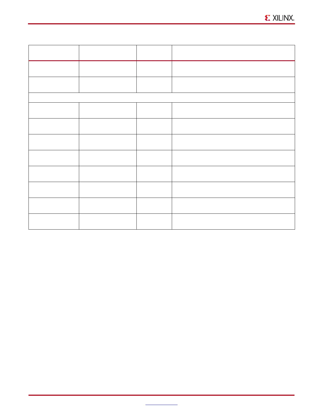
Table 4-20: FIFO Timing Parameters (Continued)
Parameter Function
Control
Signal
Description
 Loading...


