Virtex-5 FPGA User Guide www.xilinx.com 219
UG190 (v5.0) June 19, 2009
SelectIO Resources General Guidelines
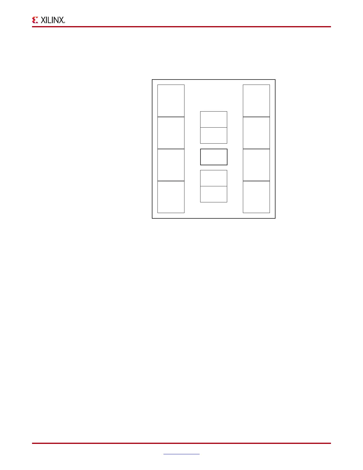
depends upon the device size, and in larger devices, there are additional full-sized banks in
the center column. In the Virtex-5 Family Overview the total number of I/O banks is listed
by device type. The XC5VLX30 has 12 usable I/O banks and one configuration bank.
Figure 6-3 is an example of a columnar floorplan showing the XC5VLX30 I/O banks.
Reference Voltage (V
REF
) Pins
Low-voltage, single-ended I/O standards with a differential amplifier input buffer require
an input reference voltage (V
REF
). V
REF
is an external input into Virtex-5 devices. Within
each I/O bank, one of every 20 I/O pins is automatically configured as a V
REF
input, if
using a single-ended I/O standard that requires a differential amplifier input buffer.
Output Drive Source Voltage (V
CCO
) Pins
Many of the low-voltage I/O standards supported by Virtex-5 devices require a different
output drive voltage (V
CCO
). As a result, each device often supports multiple output drive
source voltages.
Output buffers within a given V
CCO
bank must share the same output drive source
voltage. The following input buffers use the V
CCO
voltage: LVTTL, LVCMOS, PCI, LVDCI
and other DCI standards.
X-Ref Target - Figure 6-3
Figure 6-3: Virtex-5 FPGA XC5VLX30 I/O Banks
ug190_6_03_021306
BANK
40 I/O
BANK
20 I/O
BANK
20 I/O
BANK
20 I/O
BANK
20 I/O
BANK
40 I/O
BANK
40 I/O
BANK
40 I/O
CONFIG
BANK
40 I/O
BANK
40 I/O
BANK
40 I/O
BANK
40 I/O
 Loading...


