Virtex-5 FPGA User Guide www.xilinx.com 107
UG190 (v5.0) June 19, 2009
PLL Use Models
In some cases precise alignment will not occur because of the difference in loading between
the input capacitance of the external component and the feedback path capacitance of the
FPGA. For example, the external components can have an input capacitance on 1 pF to
4 pF while the FPGA has an input capacitance of around 8 pF. There is a difference in the
signal slope, which is basically skew. Designers need to be aware of this effect to ensure
timing.
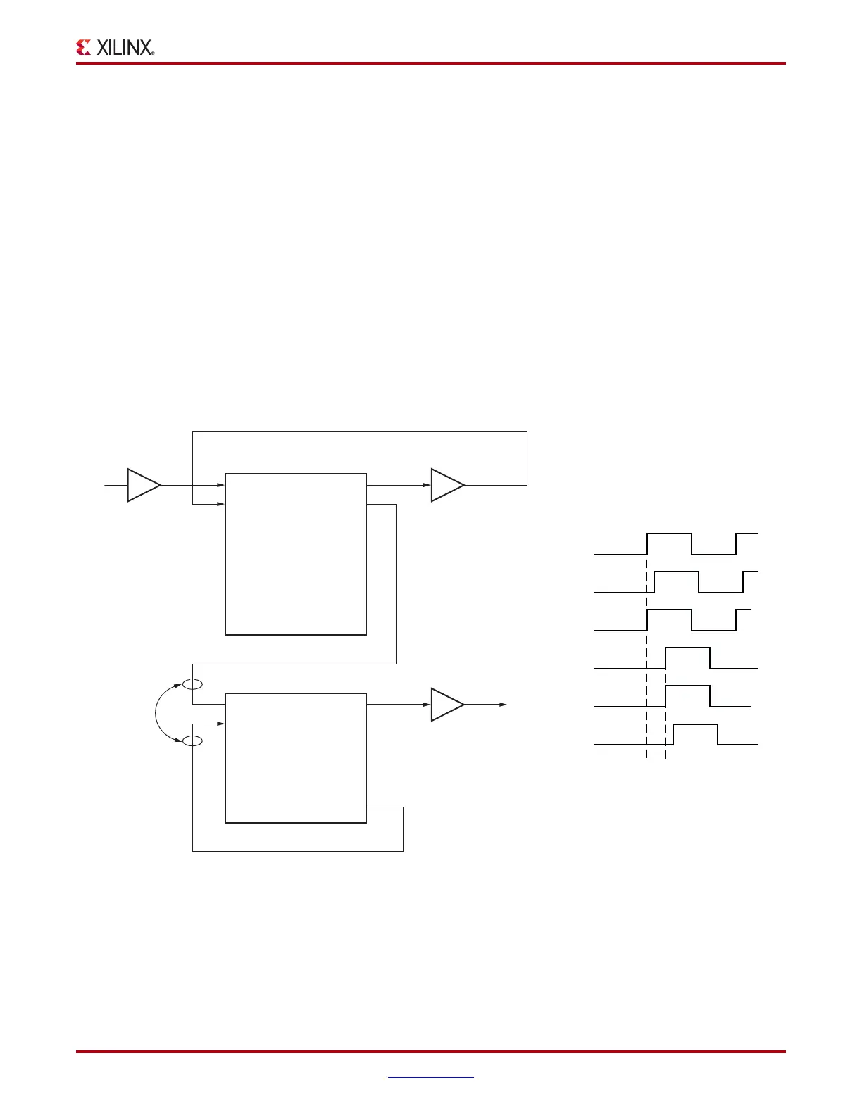
DCM Driving PLL
The DCM provides an excellent method for generating precision phase-shifted clocks.
However, the DCM cannot reduce the jitter on the reference clock. The PLL can be used to
reduce the output jitter of one DCM clock output. This configuration is shown in
Figure 3-13. The PLL is configured to not introduce any phase shift (zero delay through the
PLL). The associated waveforms are shown to the right of the block diagram. When the
output of the DCM is used to drive the PLL directly, both DCM and PLL must reside within
the same CMT block. This is the preferred implementation since it produces a minimal
amount of noise on the local, dedicated route. However, a connection can also be made by
connecting the DCM to a BUFG and then to the CLKIN input of a PLL.
X-Ref Target - Figure 3-13
Figure 3-13: DCM Driving a PLL
CLKIN
RST
IBUFG
12
3
4
5
6
BUFG
BUFG
To Logic, etc.
CLK0
CLK180
CLK270
CLK2X
CLK2X180
CLKDV
CLKFX
CLKFX180
CLK90
DCM
CLKFBIN
PLL
ug190_3_13_092107
CLKIN1
Matches
RST
CLKFBIN
CLKOUT0
CLKOUT2
CLKOUT3
CLKOUT4
CLKOUT5
CLKFBOUT
CLKOUT1
1
2
3
4
5
6
 Loading...


