294 www.xilinx.com Virtex-5 FPGA User Guide
UG190 (v5.0) June 19, 2009
Chapter 6: SelectIO Resources
Differential Termination: DIFF_TERM Attribute
Virtex-5 FPGA IOBs provide a 100Ωdifferential termination across the input differential
receiver terminals. This attribute is used in conjunction with LVDS_25, LVDSEXT_25,
HT_25, and RSDS_25. HT_25 replaces the Virtex-4 FPGA LDT_25 standard.
The on-chip input differential termination in Virtex-5 devices provides major advantages
over the external resistor by removing the stub at the receiver completely and therefore
greatly improving signal integrity:
• Consumes less power than DCI termination
• Does not use VRP/VRN pins (DCI)
The V
CCO
of the I/O bank must be connected to 2.5V ±5% to provide 100Ω of effective
differential termination. DIFF_TERM is only available for inputs and can only be used with
a bank voltage of V
CCO
=2.5V. The “Differential Termination Attribute” (DIFF_TERM)
section outlines using this feature.
LVDS and Extended LVDS (Low Voltage Differential Signaling)
Low Voltage Differential Signaling (LVDS) is a very popular and powerful high-speed
interface in many system applications. Virtex-5 FPGA I/Os are designed to comply with
the EIA/TIA electrical specifications for LVDS to make system and board design easier.
With the use of an LVDS current-mode driver in the IOBs, the need for external source
termination in point-to-point applications is eliminated, and with the choice of an
extended mode, Virtex-5 devices provide the most flexible solution for doing an LVDS
design in an FPGA.
Extended LVDS provides a higher drive capability and voltage swing (350 - 750 mV),
making it ideal for long-distance or cable LVDS links. The output AC characteristics of the
LVDS extended mode driver are not within the EIA/TIA specifications. The LVDS
extended mode driver is intended for situations requiring higher drive capabilities to
produce an LVDS signal within the EIA/TIA specification at the receiver.
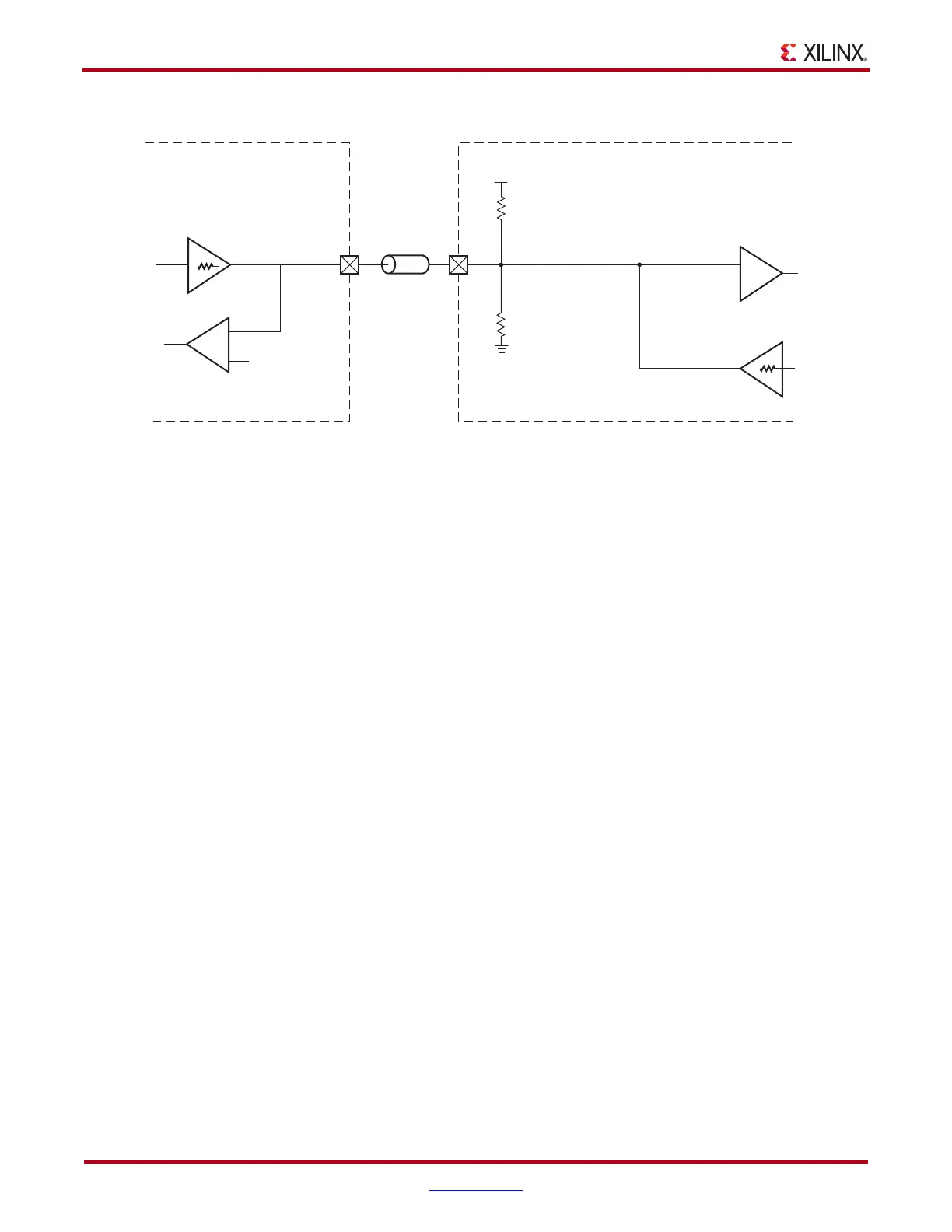
X-Ref Target - Figure 6-86
Figure 6-86: SSTL18_II_T_DCI (1.8V) Split-Thevenin Termination
ug190_6_93_041206
Z
0
IOB
IOB
SSTL18_II_T_DCI
SSTL18_II_T_DCI
V
CCO
= 1.8V
2R
VRP
= 2Z
0
= 100Ω
2R
VRN
= 2Z
0
= 100Ω
V
REF
= 0.9V
+
–
DCI Not 3-stated 3-stated
R
0
= 20Ω
V
REF
= 0.9V
R
0
= 20Ω
 Loading...


