36 www.xilinx.com Virtex-5 FPGA User Guide
UG190 (v5.0) June 19, 2009
Chapter 1: Clock Resources
Additional Use Models
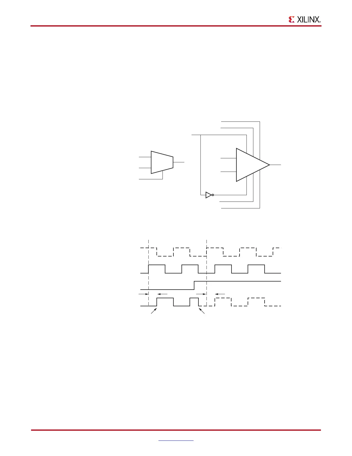
Asynchronous Mux Using BUFGCTRL
In some cases an application requires immediate switching between clock inputs or
bypassing the edge sensitivity of BUFGCTRL. An example is when one of the clock inputs
is no longer switching. If this happens, the clock output would not have the proper
switching conditions because the BUFGCTRL never detected a clock edge. This case uses
the asynchronous mux. Figure 1-13 illustrates an asynchronous mux with BUFGCTRL
design example. Figure 1-14 shows the asynchronous mux timing diagram.
In Figure 1-14:
• The current clock is from I0.
• S is activated High.
• The Clock output immediately switches to I1.
• When Ignore signals are asserted High, glitch protection is disabled.
X-Ref Target - Figure 1-13
Figure 1-13: Asynchronous Mux with BUFGCTRL Design Example
X-Ref Target - Figure 1-14
Figure 1-14: Asynchronous Mux Timing Diagram
IGNORE1
IGNORE0
CE1
S
CE0
S1
S0
I1
I0
S
I1
I0
O
Asynchronous MUX
Design Example
ug190_1_13_032306
V
DD
V
DD
V
DD
V
DD
O
UG190_1_14_032306
T
BCCKO_O
T
BCCKO_O
I0
I1
S
O
at I0 Begin I1
 Loading...


