370 www.xilinx.com Virtex-5 FPGA User Guide
UG190 (v5.0) June 19, 2009
Chapter 8: Advanced SelectIO Logic Resources
Output Parallel-to-Serial Logic Resources (OSERDES)
The OSERDES in Virtex-5 devices is a dedicated parallel-to-serial converter with specific
clocking and logic resources designed to facilitate the implementation of high-speed
source-synchronous interfaces. Every OSERDES module includes a dedicated serializer for
data and 3-state control. Both Data and 3-state serializers can be configured in SDR and
DDR mode. Data serialization can be up to 6:1 (10:1 if using “OSERDES Width
Expansion”). 3-state serialization can be up to 4:1.
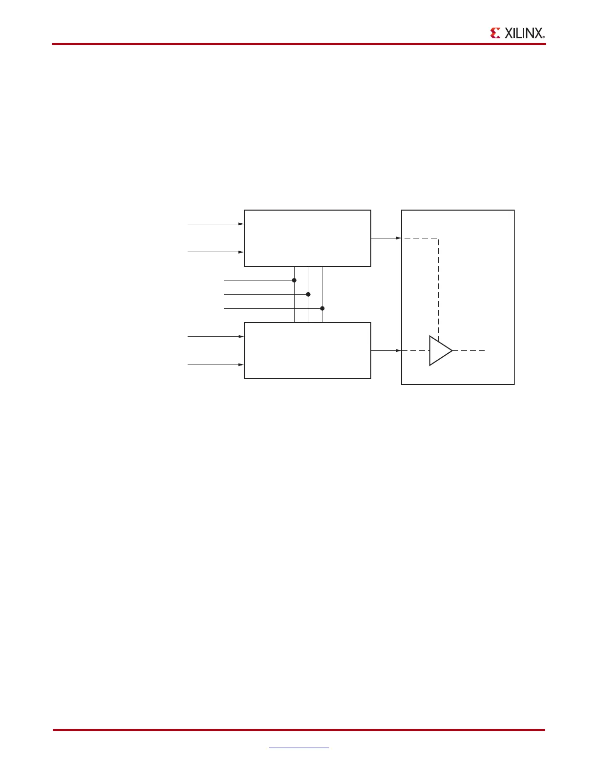
Figure 8-14 shows a block diagram of the OSERDES, highlighting all the major
components and features of the block.
Data Parallel-to-Serial Converter
The data parallel-to-serial converter in one OSERDES blocks receives two to six bits of
parallel data from the fabric (10:1 if using “OSERDES Width Expansion”), serializes the
data, and presents it to the IOB via the OQ outputs. Parallel data is serialized from lowest
order data input pin to highest (i.e., data on the D1 input pin is the first bit transmitted at
the OQ pins). The data parallel-to-serial converter is available in two modes: single-data
rate (SDR) and double-data rate (DDR).
The OSERDES uses two clocks, CLK and CLKDIV, for data rate conversion. CLK is the
high-speed serial clock, CLKDIV is the divided parallel clock. It is assumed that CLK and
CLKDIV are phase aligned.
Prior to use, a reset must be applied to the OSERDES. The OSERDES contains an internal
counter that controls dataflow. Failure to synchronize the reset with the CLKDIV will
produce an unexpected output. Table 8-5 describes the relationship between CLK and
CLKDIV in all modes.
X-Ref Target - Figure 8-14
Figure 8-14: OSERDES Block Diagram
3-State
Parallel-to-Serial Converter
Data
Parallel-to-Serial Converter
CLK
CLKDIV
SR
D1 - D6
OCE
TCE
T1 - T4
TQ
IOB
OQ
ug190_8_14_100307
Output Driver
 Loading...


