Virtex-5 FPGA User Guide www.xilinx.com 165
UG190 (v5.0) June 19, 2009
Built-in Error Correction
ECC Modes of Operation
There are three types of ECC operation: standard, encode only, and decode only. The
standard ECC mode uses both the encoder and decoder.
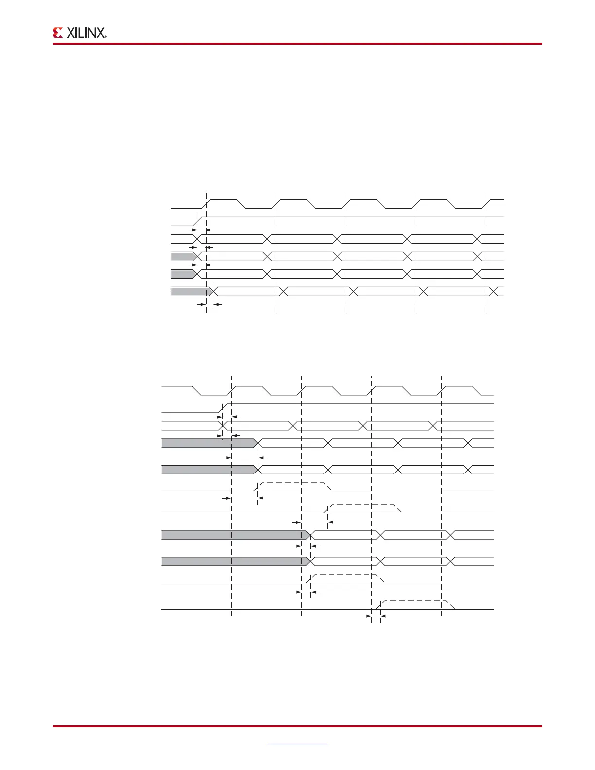
The various modes of ECC operation in both block RAM and FIFO are shown in
Figure 4-31 and Figure 4-32. The block RAM WRADDR and RDADDR address inputs are
supplied by the user. The FIFO WRADDR and RDADDR addresses are generated
internally from the write counter and read counter.
X-Ref Target - Figure 4-31
Figure 4-31: ECC Write Operation
WREN
WRCLK
WRADDR[8:0]
DI[63:0]
DIP[7:0]
(Decode Only Mode)
ECCPARITY[7:0]
abcd
A
B
C
D
PC PDPB
PA
PC PDPB
PA
TRCCK_EN
TRCCK_ADDR
TRCCK_DI_ECC
ug190_4_32_022307
TRCKO_ECC_PARITY
T1W T2W T3W T4W T5W
X-Ref Target - Figure 4-32
Figure 4-32: ECC Read Operation
RDEN
RDADDR[8:0]
RDCLK
DO[63:0]
(Latch Mode)
DOP[7:0]
(Latch Mode)
SBITERR
(Register Mode)
DBITERR
(Register Mode)
abc
d
A
BC
PBPA P C
DO[63:0]
(Register Mode)
DOP[7:0]
(Register Mode)
A
BC
PBPA P C
TRCCK_EN
TRCCK_ADDR
TRCKO_DO (Register Mode)
TRCKO_DO (Latch Mode)
TRCKO_ECC_SBITERR (Latch Mode)
TRCKO_ECC_DBITERR (Latch Mode)
Single Bit Error
Double Bit Error
ug190_4_33_020707
T1R T2R T3R T4R
TRCKO_ECC_SBITERR (Register Mode)
TRCKO_ECC_DBITERR (Register Mode)
SBITERR
(Latch Mode)
DBITERR
(Latch Mode)
Single Bit Error
Double Bit Error
 Loading...


