90 www.xilinx.com Virtex-5 FPGA User Guide
UG190 (v5.0) June 19, 2009
Chapter 3: Phase-Locked Loops (PLLs)
Phase Locked Loop (PLL)
Virtex-5 devices contain up to six CMT tiles. The PLLs main purpose is to serve as a
frequency synthesizer for a wide range of frequencies, and to serve as a jitter filter for
either external or internal clocks in conjunction with the DCMs of the CMT.
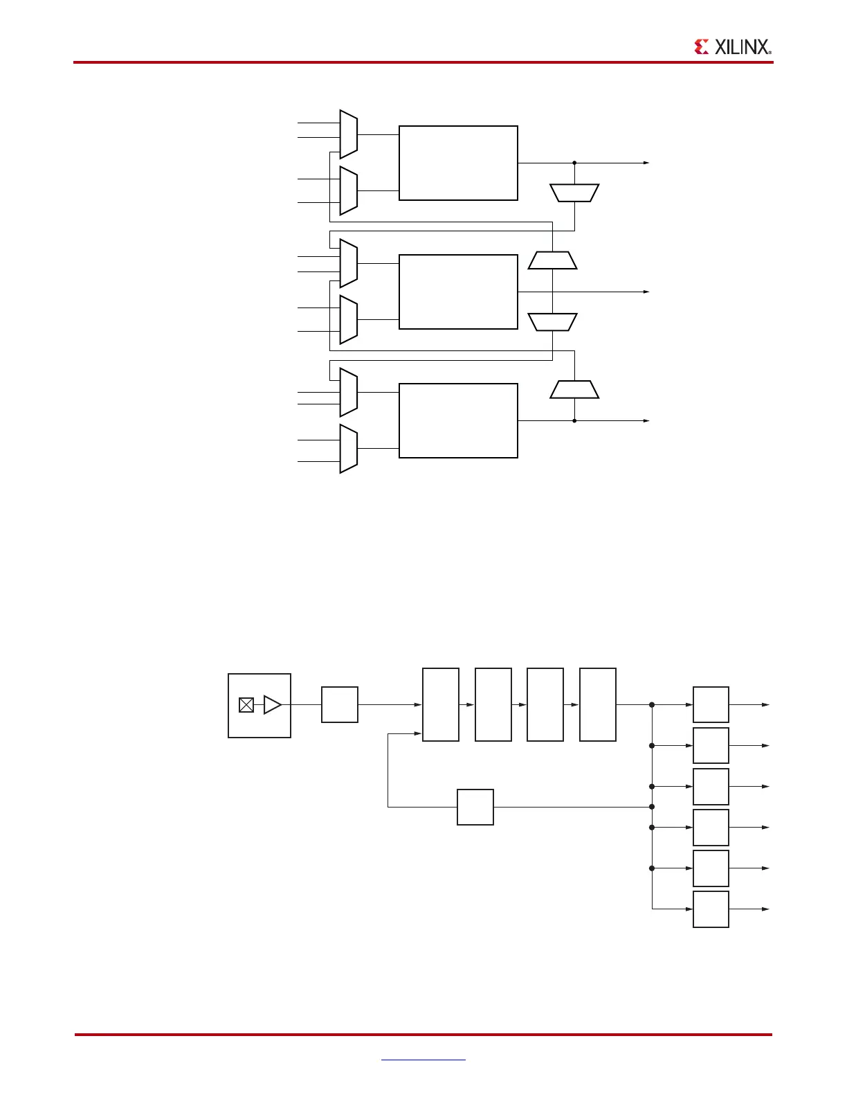
The PLL block diagram shown in Figure 3-2 provides a general overview of the PLL
components.
X-Ref Target - Figure 3-1
Figure 3-1: Block Diagram of the Virtex-5 FPGA CMT
From any IBUFG implementation
From any BUFG implementation
DCM1
DCM2
PLL
clkout_pll<5:0>
To any BUFG
implementation
To any BUFG
implementation
To any BUFG
implementation
UG190_c3_01_022709
X-Ref Target - Figure 3-2
Figure 3-2: Block Diagram of the Virtex-5 FPGA PLL
Clock Pin
D
M
PFD CP LF VCO O0
O1
O2
O3
O4
O5
ug190_3_02_030506
 Loading...


