98 www.xilinx.com Virtex-5 FPGA User Guide
UG190 (v5.0) June 19, 2009
Chapter 3: Phase-Locked Loops (PLLs)
PLL Attributes
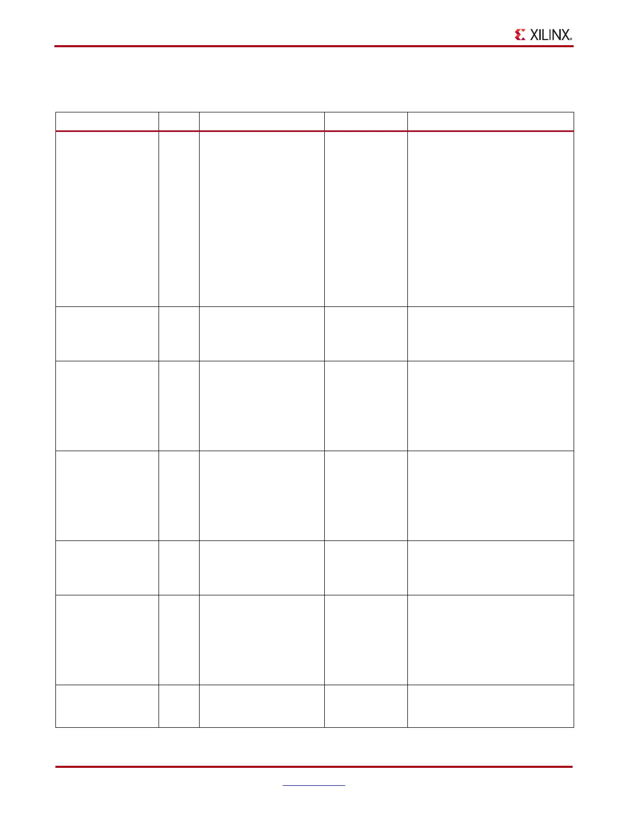
Table 3-4: PLL Attributes
Attribute Type Allowed Values Default Description
COMPENSATION String
SYSTEM_SYNCHRONOUS
SOURCE_SYNCHRONOUS
SYSTEM_
SYNCHRONOUS
Specifies the PLL phase
compensation for the incoming clock.
SYSTEM_SYNCHRONOUS
attempts to compensate all clock
delay for 0 hold time.
SOURCE_SYNCHRONOUS is used
when a clock is provided with data
and thus phased with the clock.
Additional attributes automatically
selected by the ISE software:
INTERNAL
EXTERNAL
DCM2PLL
PLL2DCM
BANDWIDTH String HIGH
LOW
OPTIMIZED
OPTIMIZED Specifies the PLL programming
algorithm affecting the jitter, phase
margin and other characteristics of
the PLL.
CLKOUT[0:5]_DIVIDE
Integer 1 to 128 1 Specifies the amount to divide the
associated CLKOUT clock output if a
different frequency is desired. This
number in combination with the
CLKFBOUT_MULT and
DIVCLK_DIVIDE values will
determine the output frequency.
CLKOUT[0:5]_PHASE
Real –360.0 to 360.0 0.0 Allows specification of the output
phase relationship of the associated
CLKOUT clock output in number of
degrees offset (i.e., 90 indicates a 90°
or ¼ cycle offset phase offset while
180 indicates a 180° offset or ½ cycle
phase offset).
CLKOUT[0:5]_
DUTY_CYCLE
Real 0.01 to 0.99 0.50 Specifies the Duty Cycle of the
associated CLKOUT clock output in
percentage (i.e., 0.50 will generate a
50% duty cycle).
CLKFBOUT_MULT Integer 1 to 64 1 Specifies the amount to multiply all
CLKOUT clock outputs if a different
frequency is desired. This number, in
combination with the associated
CLKOUT#_DIVIDE value and
DIVCLK_DIVIDE value, will
determine the output frequency.
DIVCLK_DIVIDE Integer 1 to 52 1 Specifies the division ratio for all
output clocks with respect to the
input clock.
 Loading...


