Virtex-5 FPGA User Guide www.xilinx.com 295
UG190 (v5.0) June 19, 2009
Specific Guidelines for I/O Supported Standards
Transmitter Termination
The Virtex-5 FPGA LVDS transmitter does not require any external termination. Table 6-36
lists the allowed attributes corresponding to the Virtex-5 FPGA LVDS current-mode
drivers. Virtex-5 FPGA LVDS current-mode drivers are a true current source and produce
the proper (EIA/TIA compliant) LVDS signal.
Receiver Termination
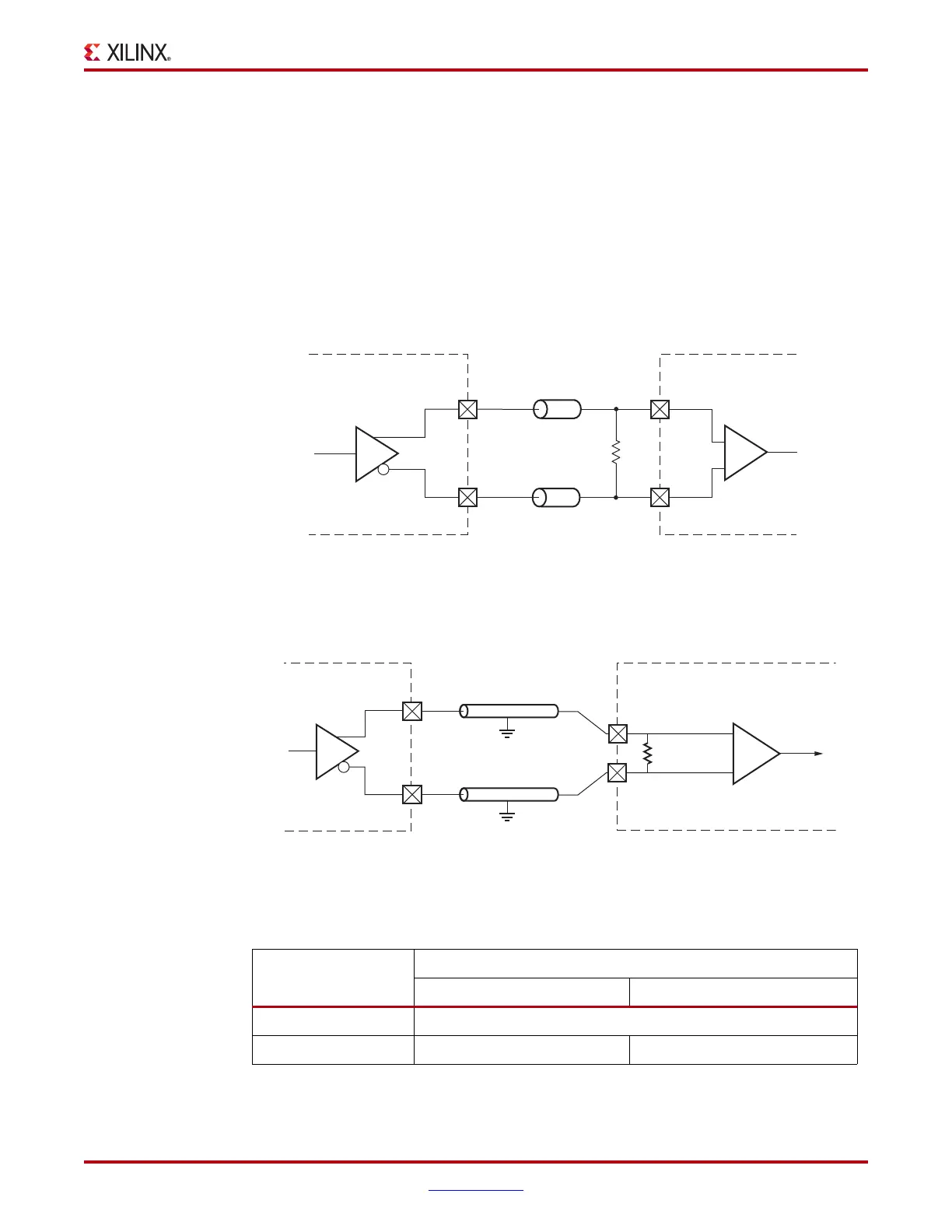
Figure 6-87 is an example of differential termination for an LVDS receiver on a board with
50 Ω transmission lines.
Figure 6-88 is an example of a differential termination for an LVDS receiver on a board with
50 Ω transmission lines.
Table 6-36 lists the available Virtex-5 FPGA LVDS I/O standards and attributes supported.
X-Ref Target - Figure 6-87
Figure 6-87: LVDS_25 Receiver Termination
X-Ref Target - Figure 6-88
Figure 6-88: LVDS_25 With DIFF_TERM Receiver Termination
Table 6-36: Allowed Attributes of the LVDS I/O Standard
Attributes
Primitives
IBUFDS/IBUFGDS OBUFDS/OBUFTDS
IOSTANDARD LVDS_25, LVDSEXT_25
DIFF_TERM TRUE, FALSE N/A
ug190_6_81_030506
+
–
External Termination
Z
0
IOB
IOB
LVDS_25
LVDS_25
Z
0
R
DIFF
= 2Z
0
= 100Ω
ug190_6_82_030506
Data in
Z
0
= 50Ω
Z
0
= 50Ω
R
DIFF
= 100Ω
LVDS_25
LVDS_25
+
–
0
0
IOB IOB
 Loading...


