Virtex-5 FPGA User Guide www.xilinx.com 115
UG190 (v5.0) June 19, 2009
Block RAM Introduction
Block RAM Introduction
In addition to distributed RAM memory and high-speed SelectIO™ memory interfaces,
Virtex-5 devices feature a large number of 36 Kb block RAMs. Each 36 Kb block RAM
contains two independently controlled 18 Kb RAMs. Block RAMs are placed in columns,
and the total number of block RAM memory depends on the size of the Virtex-5 device.
The 36 Kb blocks are cascadable to enable a deeper and wider memory implementation,
with a minimal timing penalty.
Embedded dual- or single-port RAM modules, ROM modules, synchronous FIFOs, and
data width converters are easily implemented using the Xilinx CORE Generator™ block
memory modules. Multirate FIFOs can be generated using the CORE Generator FIFO
Generator module. The synchronous or asynchronous (multirate) FIFO implementation
does not require additional CLB resources for the FIFO control logic since it uses dedicated
hardware resources.
Synchronous Dual-Port and Single-Port RAMs
Data Flow
The true dual-port 36 Kb block RAM dual-port memories consist of a 36 Kb storage area
and two completely independent access ports, A and B. Similarly, each 18 Kb block RAM
dual-port memory consists of an 18 Kb storage area and two completely independent
access ports, A and B. The structure is fully symmetrical, and both ports are
interchangeable. Figure 4-1 illustrates the true dual-port data flow. Table 4-2 lists the port
names and descriptions.
Data can be written to either or both ports and can be read from either or both ports. Each
write operation is synchronous, each port has its own address, data in, data out, clock,
clock enable, and write enable. The read and write operations are synchronous and require
a clock edge.
There is no dedicated monitor to arbitrate the effect of identical addresses on both ports. It
is up to the user to time the two clocks appropriately. Conflicting simultaneous writes to
the same location never cause any physical damage but can result in data uncertainty.
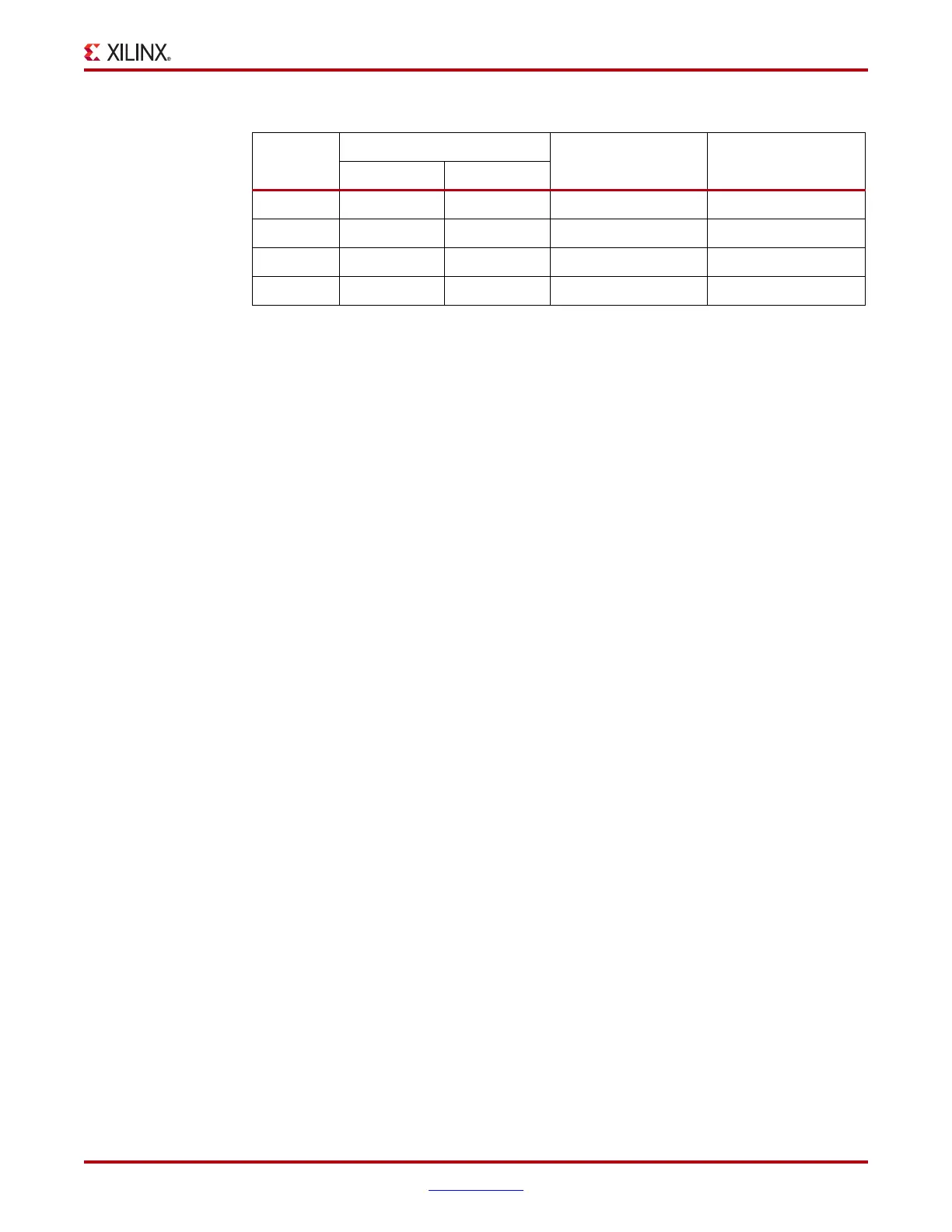
RAMB36 1, 2, or 4 9, 18, or 36 Same as setting 8, 16, or 32
RAMB36 9, 18, or 36 1, 2, or 4 8, 16, or 32 Same as setting
RAMB36 1, 2, or 4 1, 2, or 4 Same as setting Same as setting
RAMB36 9, 18, or 36 9, 18, or 36 Same as setting Same as setting
Notes:
1. Do not use parity bits DIP/DOP when one port widths is less than nine and another port width is nine
or greater.
Table 4-1: Parity Use Sceneries (Continued)
Primitive
Settings
Effective Read Width Effective Write Width
Read Width Write Width
 Loading...


