116 www.xilinx.com Virtex-5 FPGA User Guide
UG190 (v5.0) June 19, 2009
Chapter 4: Block RAM
X-Ref Target - Figure 4-1
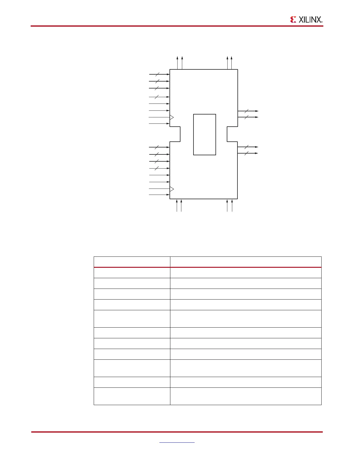
Figure 4-1: True Dual-Port Data Flows
Table 4-2: True Dual-Port Names and Descriptions
Port Name Description
DI[A|B] Data Input Bus
DIP[A|B]
(1)
Data Input Parity Bus, can be used for additional data inputs
ADDR[A|B] Address Bus
WE[A|B] Byte-wide Write Enable
EN[A|B] When inactive no data is written to the block RAM and the
output bus remains in its previous state
SSR[A|B] Synchronous Set/Reset for either latch or register modes
CLK[A|B] Clock Input
DO[A|B] Data Output Bus
DOP[A|B]
(1)
Data Output Parity Bus, can be used for additional data
outputs
REGCE[A|B] Output Register Enable
CASCADEINLAT[A|B] Cascade input pin for 64K x 1 mode when optional output
registers are not enabled
DOPA
DIPA
ADDRA
WEA
ENA
CASCADEOUTLATB
CASCADEINLATB
SSRA
CLKA
REGCEA
REGCEB
DIPB
ADDRB
WEB
ENB
SSRB
CLKB
36-Kbit Block RAM
ug0190_4_01_032106
DOPB
DOB
DOA
DIA
DIB
36 Kb
Memory
Array
Port A
Port B
CASCADEOUTLATA
CASCADEINLATA
CASCADEOUTREGBCASCADEOUTREGA
CASCADEINREGBCASCADEINREGA
 Loading...


