Virtex-5 FPGA User Guide www.xilinx.com 321
UG190 (v5.0) June 19, 2009
ILOGIC Resources
Input DDR Primitive (IDDR)
Figure 7-5 shows the block diagram of the IDDR primitive. Table 7-3 lists the IDDR port
signals. Table 7-4 describes the various attributes available and default values for the IDDR
primitive.
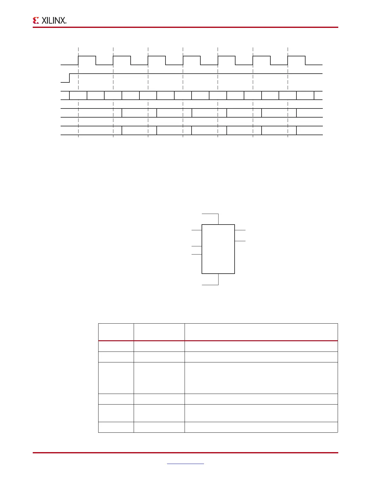
X-Ref Target - Figure 7-4
Figure 7-4: Input DDR Timing in SAME_EDGE_PIPELINED Mode
ug190_7_04_041206
C
CE
D
Q1
Q2
D0A D1A D2A
D0A D2A D4A D6A D8A D10A
D1A D3A D5A D7A D9A D11A
D3A D4A D5A D6A D7A D8A D9A D10A D11A D12A D13A
X-Ref Target - Figure 7-5
Figure 7-5: IDDR Primitive Block Diagram
Table 7-3: IDDR Port Signals
Port
Name
Function Description
Q1 and Q2 Data outputs IDDR register outputs.
C Clock input port The C pin represents the clock input pin.
CE Clock enable port The enable pin affects the loading of data into the DDR
flip-flop. When Low, clock transitions are ignored and new
data is not loaded into the DDR flip-flop. CE must be High
to load new data into the DDR flip-flop.
D Data input (DDR) IDDR register input from IOB.
R Reset Synchronous/Asynchronous reset pin. Reset is asserted
High.
S Set Synchronous/Asynchronous set pin. Set is asserted High.
ug190_7_05_062207
C
CE
D
S
R
Q1
Q2
IDDR
 Loading...


