372 www.xilinx.com Virtex-5 FPGA User Guide
UG190 (v5.0) June 19, 2009
Chapter 8: Advanced SelectIO Logic Resources
OSERDES Ports
Table 8-6 lists the available ports in the OSERDES primitive.
Data Path Output - OQ
The OQ port is the data output port of the OSERDES module. Data at the input port D1 will
appear first at OQ. This port connects the output of the data parallel-to-serial converter to
the data input of the IOB.
3-state Control Output - TQ
This port is the 3-state control output of the OSERDES module. When used, this port
connects the output of the 3-state parallel-to-serial converter to the control/3-state input of
the IOB.
High-Speed Clock Input - CLK
This high-speed clock input drives the serial side of the parallel-to-serial converters.
Divided Clock Input - CLKDIV
This divided high-speed clock input drives the parallel side of the parallel-to-serial
converters. This clock is the divided version of the clock connected to the CLK port.
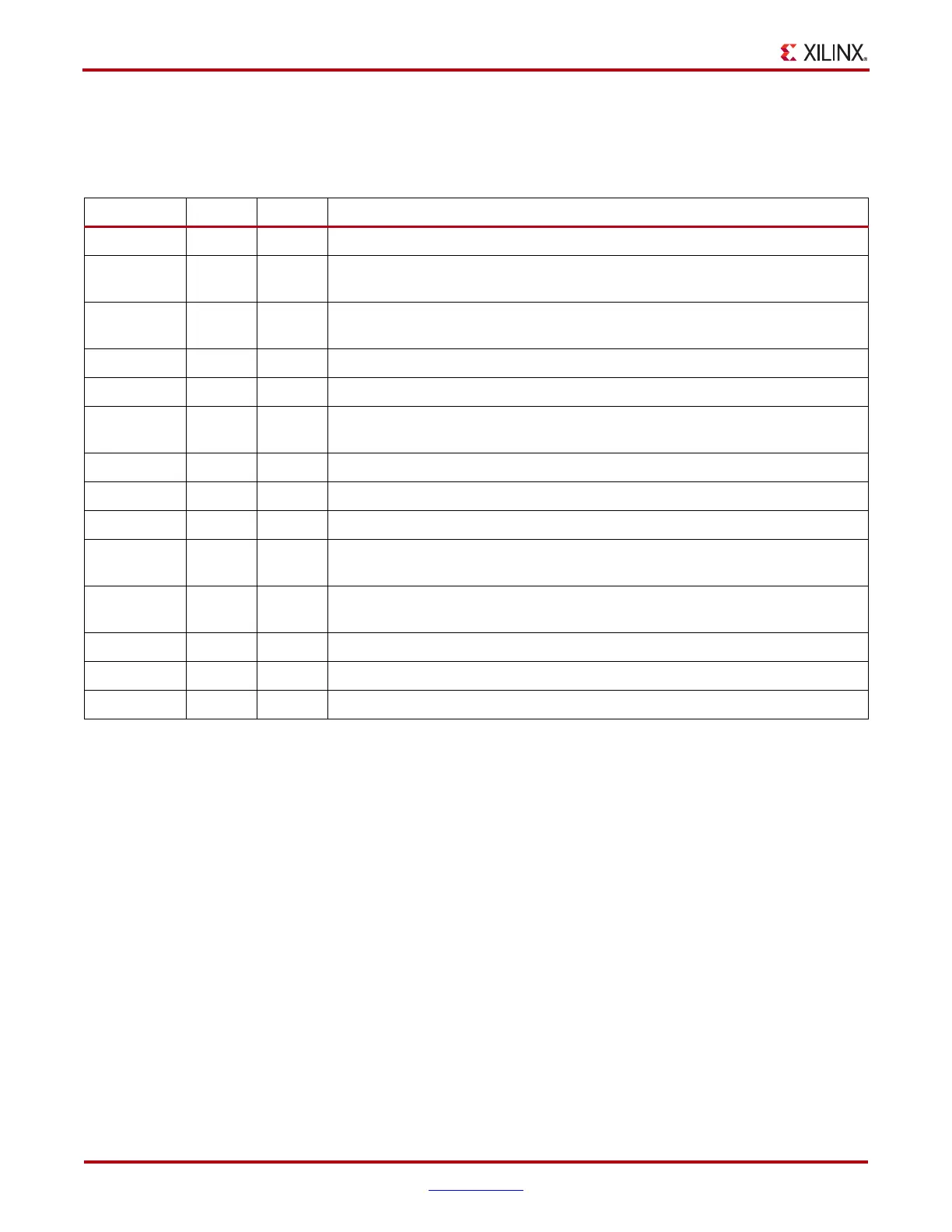
Table 8-6: OSERDES Port List and Definitions
Port Name Type Width Description
OQ Output 1 Data path output. See “Data Path Output - OQ.”
SHIFTOUT1 Output 1 Carry out for data width expansion. Connect to SHIFTIN1 of master OSERDES.
See “OSERDES Width Expansion.”
SHIFTOUT2 Output 1 Carry out for data width expansion. Connect to SHIFTIN2 of master OSERDES.
See “OSERDES Width Expansion.”
TQ Output 1 3-state control output. See “3-state Control Output - TQ.”
CLK Input 1 High-speed clock input. See “High-Speed Clock Input - CLK.”
CLKDIV Input 1 Divided clock input. Clocks delay element, deserialized data, Bitslip submodule,
and CE unit. See “Divided Clock Input - CLKDIV.”
D1 – D6 Input 1 (each) Parallel data inputs. See “Parallel Data Inputs - D1 to D6.”
OCE Input 1 Output data clock enable. See “Output Data Clock Enable - OCE.”
REV Input 1 Reverse SR pin. Not available in the OSERDES block.
SHIFTIN1 Input 1 Carry input for data width expansion. Connect to SHIFTOUT1 of slave OSERDES.
See “OSERDES Width Expansion.”
SHIFTIN2 Input 1 Carry input for data width expansion. Connect to SHIFTOUT2 of slave OSERDES.
See “OSERDES Width Expansion.”
SR Input 1 Active High reset.
T1 to T4 Input 1 (each) Parallel 3-state inputs. See “Parallel 3-state Inputs - T1 to T4.”
TCE Input 1 3-state clock enable. See “3-state Signal Clock Enable - TCE.”
 Loading...


