Virtex-5 FPGA User Guide www.xilinx.com 205
UG190 (v5.0) June 19, 2009
CLB / Slice Timing Models
Distributed RAM Timing Parameters
Table 5-8 shows the timing parameters for the distributed RAM in SLICEM for a majority
of the paths in Figure 5-27.
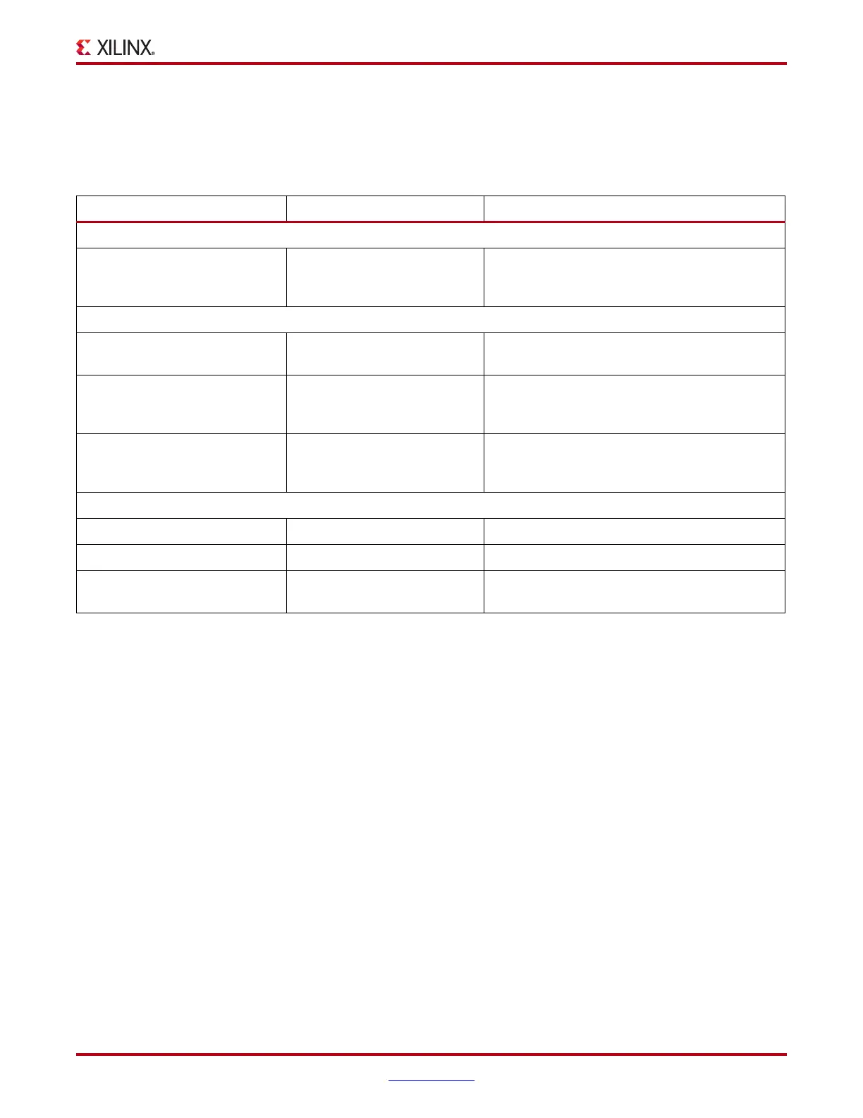
Table 5-8: Distributed RAM Timing Parameters
Parameter Function Description
Sequential Delays for a Slice LUT Configured as RAM (Distributed RAM)
T
SHCKO
(1)
CLK to A/B/C/D outputs Time after the CLK of a write operation that the
data written to the distributed RAM is stable on
the A/B/C/D output of the slice.
Setup and Hold Times for a Slice LUT Configured as RAM (Distributed RAM)
(2)
T
DS
/T
DH
(3)
AX/BX/CX/DX configured as
data input (DI1)
Time before/after the clock that data must be
stable at the AX/BX/CX/DX input of the slice.
T
ACK
/T
CKA
A/B/C/D address inputs Time before/after the clock that address signals
must be stable at the A/B/C/D inputs of the slice
LUT (configured as RAM).
T
WS
/T
WH
WE input Time before/after the clock that the write enable
signal must be stable at the WE input of the slice
LUT (configured as RAM).
Clock CLK
T
WPH
Minimum Pulse Width, High
T
WPL
Minimum Pulse Width, Low
T
WC
Minimum clock period to meet address write
cycle time.
Notes:
1. This parameters includes a LUT configured as a two-bit distributed RAM.
2. T
XXCK
= Setup Time (before clock edge), and T
CKXX
= Hold Time (after clock edge).
3. Parameter includes AI/BI/CI/DI configured as a data input (DI2).
 Loading...


