Virtex-5 FPGA User Guide www.xilinx.com 203
UG190 (v5.0) June 19, 2009
CLB / Slice Timing Models
Timing Characteristics
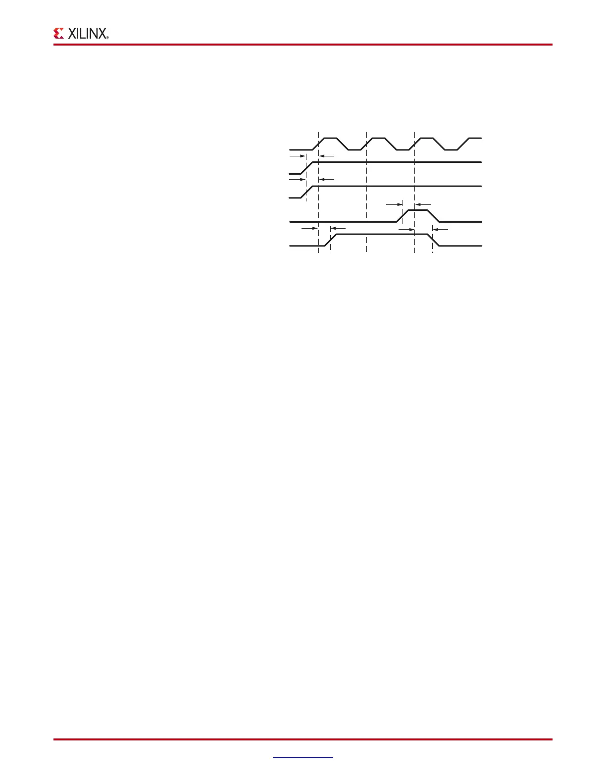
Figure 5-26 illustrates the general timing characteristics of a Virtex-5 FPGA slice.
• At time T
CEO
before clock event (1), the clock-enable signal becomes valid-High at the
CE input of the slice register.
• At time T
DICK
before clock event (1), data from either AX, BX, CX, or DX inputs
become valid-High at the D input of the slice register and is reflected on either the
AQ, BQ, CQ, or DQ pin at time T
CKO
after clock event (1).
• At time T
SRCK
before clock event (3), the SR signal (configured as synchronous reset)
becomes valid-High, resetting the slice register. This is reflected on the AQ, BQ, CQ,
or DQ pin at time T
CKO
after clock event (3).
X-Ref Target - Figure 5-26
Figure 5-26: General Slice Timing Characteristics
ug190_5_26_050506
T
CEO
123
CLK
CE
AX/BX/CX/DX
( DATA)
SR (RESET)
AQ/BQ/CQ/DQ
(OUT)
T
DICK
T
CKO
T
SRCK
T
CKO
 Loading...


