348 www.xilinx.com Virtex-5 FPGA User Guide
UG190 (v5.0) June 19, 2009
Chapter 7: SelectIO Logic Resources
ODDR VHDL and Verilog Templates
The Libraries Guide includes templates for instantiation of the ODDR module in VHDL
and Verilog.
OLOGIC Timing Models
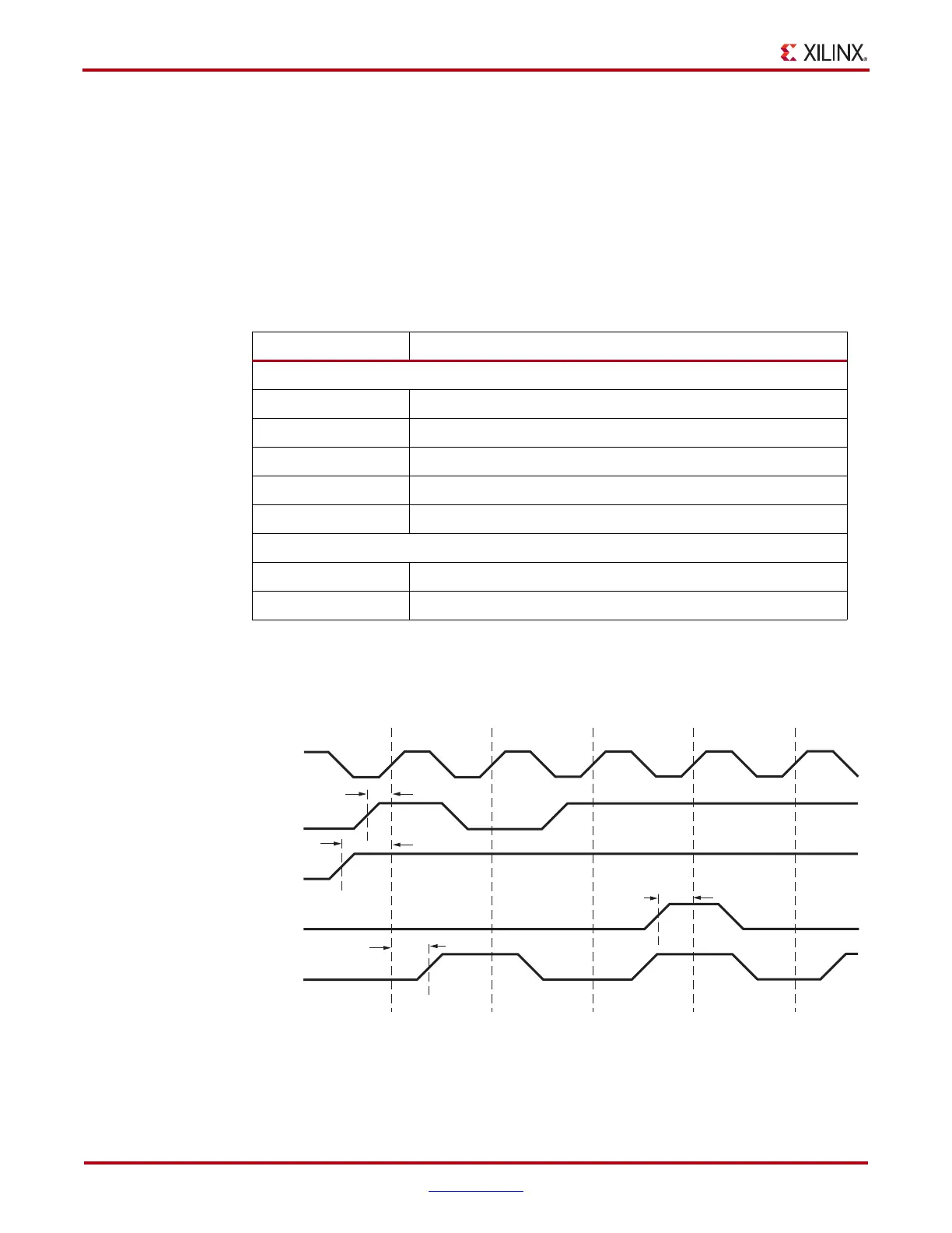
This section discusses all timing models associated with the OLOGIC block. Table 7-15
describes the function and control signals of the OLOGIC switching characteristics in the
Virtex-5 FPGA Data Sheet.
Timing Characteristics
Figure 7-26 illustrates the OLOGIC output register timing.
Table 7-15: OLOGIC Switching Characteristics
Symbol Description
Setup/Hold
T
ODCK
/T
OCKD
D1/D2 pins Setup/Hold with respect to CLK
T
OOCECK
/T
OCKOCE
OCE pin Setup/Hold with respect to CLK
T
OSRCK
/T
OCKSR
SR/REV pin Setup/Hold with respect to CLK
T
OTCK
/T
OCKT
T1/T2 pins Setup/Hold with respect to CLK
T
OTCECK
/T
OCKTCE
TCE pin Setup/Hold with respect to CLK
Clock to Out
T
OCKQ
CLK to OQ/TQ out
T
RQ
SR/REV pin to OQ/TQ out
X-Ref Target - Figure 7-26
Figure 7-26: OLOGIC Output Register Timing Characteristics
12345
CLK
D1
OCE
SR
OQ
T
OCKQ
T
ODCK
T
OOCECK
T
OSRCK
ug190_7_21_041206
 Loading...


