Virtex-5 FPGA User Guide www.xilinx.com 349
UG190 (v5.0) June 19, 2009
OLOGIC Resources
Clock Event 1
• At time T
OOCECK
before Clock Event 1, the output clock enable signal becomes valid-
High at the OCE input of the output register, enabling the output register for
incoming data.
• At time T
ODCK
before Clock Event 1, the output signal becomes valid-High at the D1
input of the output register and is reflected at the OQ output at time T
OCKQ
after
Clock Event 1.
Clock Event 4
At time T
OSRCK
before Clock Event 4, the SR signal (configured as synchronous reset in this
case) becomes valid-High, resetting the output register and reflected at the OQ output at
time T
RQ
after Clock Event 4.
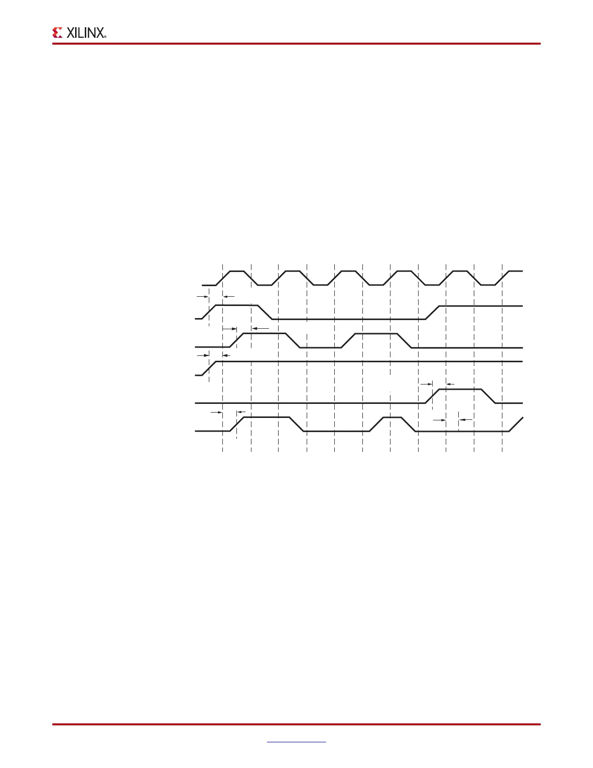
Figure 7-27 illustrates the OLOGIC ODDR register timing.
Clock Event 1
• At time T
OOCECK
before Clock Event 1, the ODDR clock enable signal becomes valid-
High at the OCE input of the ODDR, enabling ODDR for incoming data. Care must be
taken to toggle the OCE signal of the ODDR register between the rising edges and
falling edges of CLK as well as meeting the register setup-time relative to both clock
edges.
• At time T
ODCK
before Clock Event 1 (rising edge of CLK), the data signal D1 becomes
valid-High at the D1 input of ODDR register and is reflected on the OQ output at time
T
OCKQ
after Clock Event 1.
Clock Event 2
• At time T
ODCK
before Clock Event 2 (falling edge of CLK), the data signal D2 becomes
valid-High at the D2 input of ODDR register and is reflected on the OQ output at time
T
OCKQ
after Clock Event 2 (no change at the OQ output in this case).
X-Ref Target - Figure 7-27
Figure 7-27: OLOGIC ODDR Register Timing Characteristics
1234567891011
T
ODCK
T
OOCECK
T
ODCK
T
OSRCK
T
RQ
CLK
D1
D2
OCE
SR
OQ
T
OCKQ
ug190_7_22_012407
 Loading...


