134 www.xilinx.com Virtex-5 FPGA User Guide
UG190 (v5.0) June 19, 2009
Chapter 4: Block RAM
Block RAM Timing Model
This section describes the timing parameters associated with the block RAM in Virtex-5
devices (illustrated in Figure 4-14). The switching characteristics section in the Virtex-5
FPGA Data Sheet and the Timing Analyzer (TRCE) report from Xilinx software are also
available for reference.
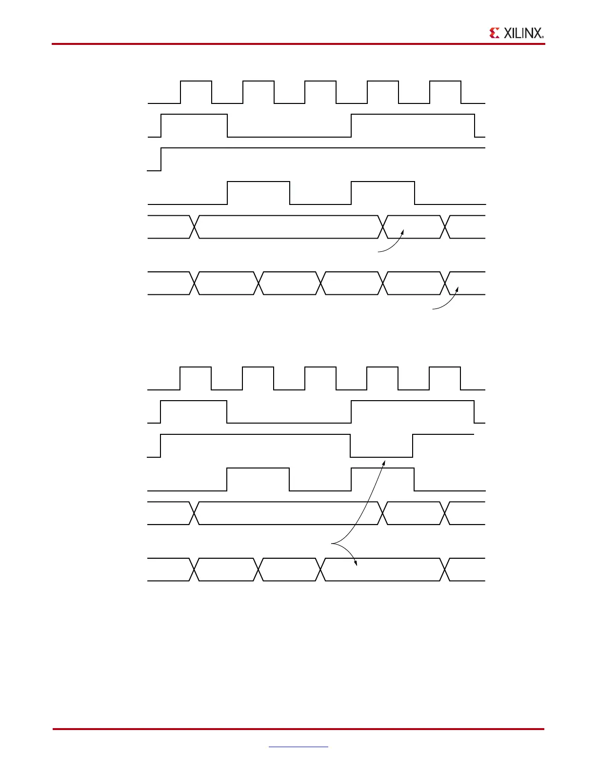
X-Ref Target - Figure 4-12
Figure 4-12: SSR Operation in Register Mode with REGCE High
CLK
RAMEN
REGCE
SSR
DBRAM
Block RAM can be read when SSR is active.
Data appears on the output of the next REGCE.
D0 D1 D2 D3
D0 SRVAL SRVALD1 D2
DO
ug190_4_29_071607
X-Ref Target - Figure 4-13
Figure 4-13: SSR Operation in Register Mode with Variable REGCE
CLK
RAMEN
REGCE
SSR
DBRAM D0 D1 D2 D3
D0 SRVAL D2D1
DO
ug190_4_29_071607
SSR only sets/resets DO when REGCE is also High.
 Loading...


