136 www.xilinx.com Virtex-5 FPGA User Guide
UG190 (v5.0) June 19, 2009
Chapter 4: Block RAM
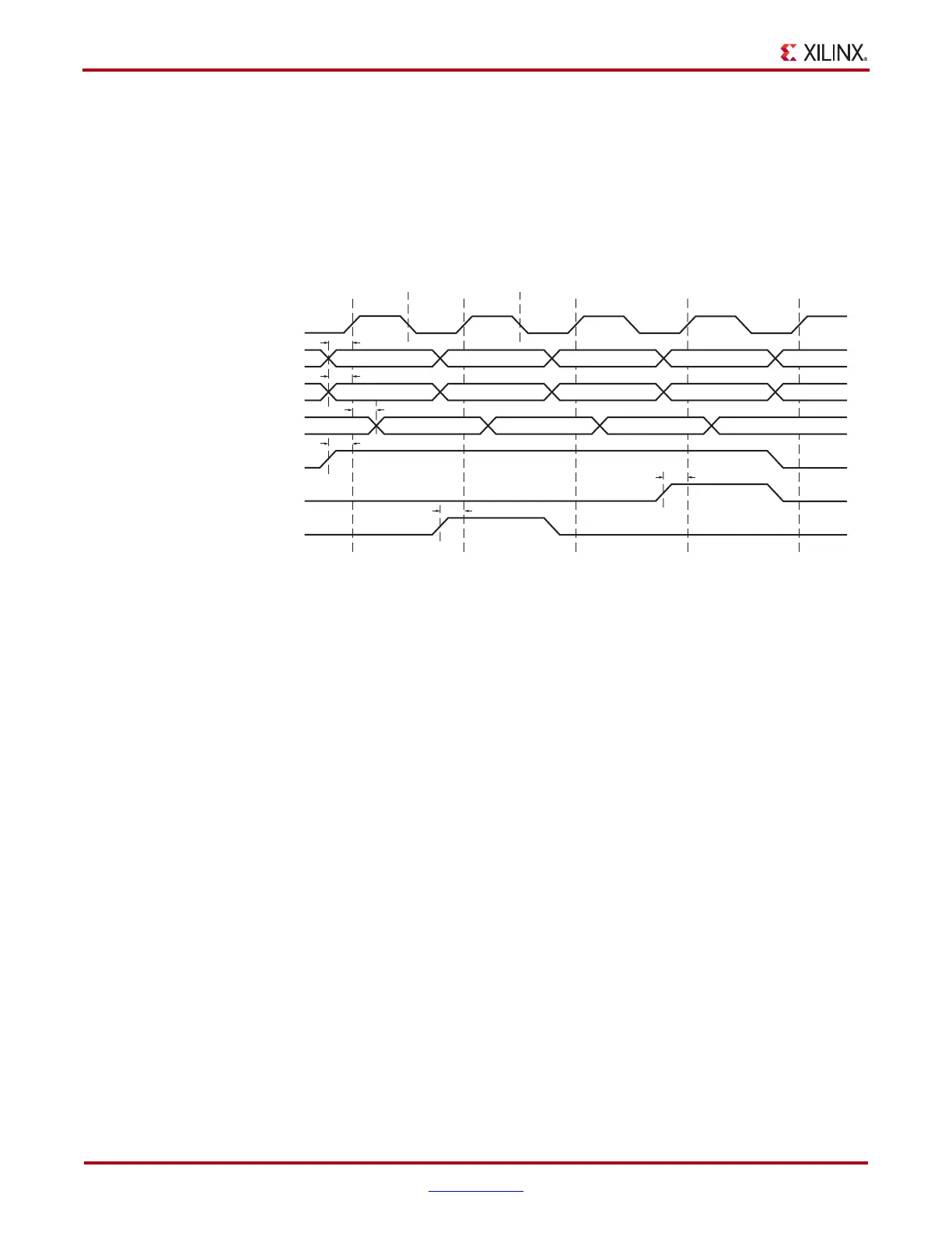
Block RAM Timing Characteristics
The timing diagram in Figure 4-14 describes a single-port block RAM in write-first mode
without the optional output register. The timing for read-first and no-change modes are
similar. For timing using the optional output register, an additional clock latency appears
at the DO pin. These waveforms correspond to latch mode when the optional output
pipeline register is not used.
At time 0, the block RAM is disabled; EN (enable) is Low.
Clock Event 1
Read Operation
During a read operation, the contents of the memory at the address on the ADDR inputs
remain unchanged.
• T
RCCK_ADDR
before clock event 1, address 00 becomes valid at the ADDR inputs of
the block RAM.
• At time T
RCCK_EN
before clock event 1, enable is asserted High at the EN input of the
block RAM, enabling the memory for the READ operation that follows.
• At time T
RCKO_DO
after clock event 1, the contents of the memory at address 00
become stable at the DO pins of the block RAM.
• Whenever EN is asserted, all address changes must meet the specified setup and hold
window. Asynchronous address changes can affect the memory content and block
RAM functionality in an unpredictable way.
X-Ref Target - Figure 4-14
Figure 4-14: Block RAM Timing Diagram
ADDR
DI
DO
EN
SSR
WE
CLK
00
DDDD
T
RCCK_ADDR
T
RDCK_DI
T
RCKO_DO
MEM (00)
T
RCCK_EN
T
RCCK_WE
Disabled DisabledRead Write Read Reset
* Write Mode = "WRITE_FIRST"
** SRVAL = 0101
0F
7E
8F 20
CCCC BBBB AAAA 0000
CCCC* MEM (7E) 0101**
ug190_4_13_022207
123 54
T
RCCK_SSR
 Loading...


