106 www.xilinx.com Virtex-5 FPGA User Guide
UG190 (v5.0) June 19, 2009
Chapter 3: Phase-Locked Loops (PLLs)
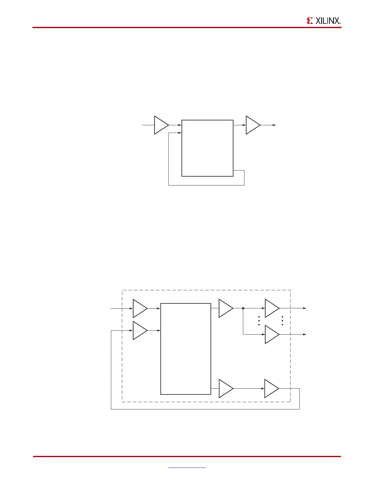
PLL with Internal Feedback
The PLL feedback can be internal to the PLL when the PLL is used as a synthesizer or jitter
filter and there is no required phase relationship between the PLL input clock and the PLL
output clock. The PLL performance should increase since the feedback clock is not
subjected to noise on the core supply since it never passes through a block powered by this
supply. Of course, noise introduced on the CLKIN signal and the BUFG will still be present
(Figure 3-11).
Zero Delay Buffer
The PLL can also be used to generate a zero delay buffer clock. A zero delay buffer can be
useful for applications where there is a single clock signal fan out to multiple destinations
with a low skew between them. This configuration is shown in the Figure 3-12. Here, the
feedback signal drives off chip and the board trace feedback is designed to match the trace
to the external components. In this configuration, it is assumed that the clock edges are
aligned at the input of the FPGA and the input of the external component. There will be a
limitation on the maximum delay allowed in the feedback path.
X-Ref Target - Figure 3-11
Figure 3-11: PLL with Internal Feedback
CLKIN1
CLKFBIN
RST
CLKOUT0
CLKOUT1
CLKOUT2
CLKOUT3
CLKOUT4
CLKOUT5
CLKFBOUT
PLL
IBUFG BUFG
To Lo g i c
UG190_3_11_040906
X-Ref Target - Figure 3-12
Figure 3-12: Zero Delay Buffer
CLKIN1
CLKFBIN
RST
CLKOUT0
CLKOUT1
CLKOUT2
CLKOUT3
CLKOUT4
CLKOUT5
CLKFBOUT
PLL
IBUFG
Inside FPGA
OBUF
To
External
Components
BUFG
BUFG
UG190_3_12_120108
 Loading...


