356 www.xilinx.com Virtex-5 FPGA User Guide
UG190 (v5.0) June 19, 2009
Chapter 8: Advanced SelectIO Logic Resources
Bitslip Operation - BITSLIP
The BITSLIP pin performs a Bitslip operation synchronous to CLKDIV when asserted
(active High). Subsequently, the data seen on the Q1 to Q6 output ports will shift, as in a
barrel-shifter operation, one position every time Bitslip is invoked (DDR operation is
different from SDR). See “BITSLIP Submodule” for more details.
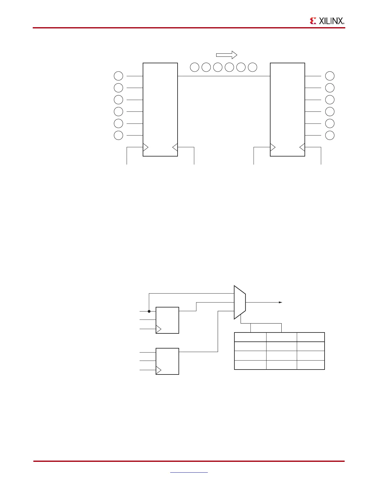
Clock Enable Inputs - CE1 and CE2
Each ISERDES_NODELAY block contains an input clock enable module (Figure 8-4).
When NUM_CE = 1, the CE2 input is not used, and the CE1 input is an active High clock
enable connected directly to the input registers in the ISERDES_NODELAY. When
NUM_CE = 2, the CE1 and CE2 inputs are both used, with CE1 enabling the
ISERDES_NODELAY for ½ of a CLKDIV cycle, and CE2 enabling the
ISERDES_NODELAY for the other ½. The internal clock enable signal ICE shown in
Figure 8-4 is derived from the CE1 and CE2 inputs. ICE drives the clock enable inputs of
X-Ref Target - Figure 8-3
Figure 8-3: Bit Ordering on Q1–Q6 Outputs of ISERDES_NODELAY Ports
F E
QD
OSERDES ISERDES
Data Bits
D1
D C B A
A
D2
B
D3
C
D4
D
D5
E
D6
Q1
Q2
Q3
Q4
Q5
Q6
F
F
E
D
C
B
A
CLKDIV_TX
CLK_TX CLK_RX CLKDIV_RX
UG190_8_03_100307
X-Ref Target - Figure 8-4
Figure 8-4: Input Clock Enable Module
D
AR
CE1R
ICE
NUM_CE ICECLKDIV
1 CE1X
2 CE2R0
2 CE1R1
(To ISERDES Input Registers)
CE1 Q
RST
CLKDIV
D
AR
CE2R
CE2 Q
RST
CLKDIV
UG190_8_04_110707
 Loading...


