318 www.xilinx.com Virtex-5 FPGA User Guide
UG190 (v5.0) June 19, 2009
Chapter 7: SelectIO Logic Resources
ILOGIC Resources
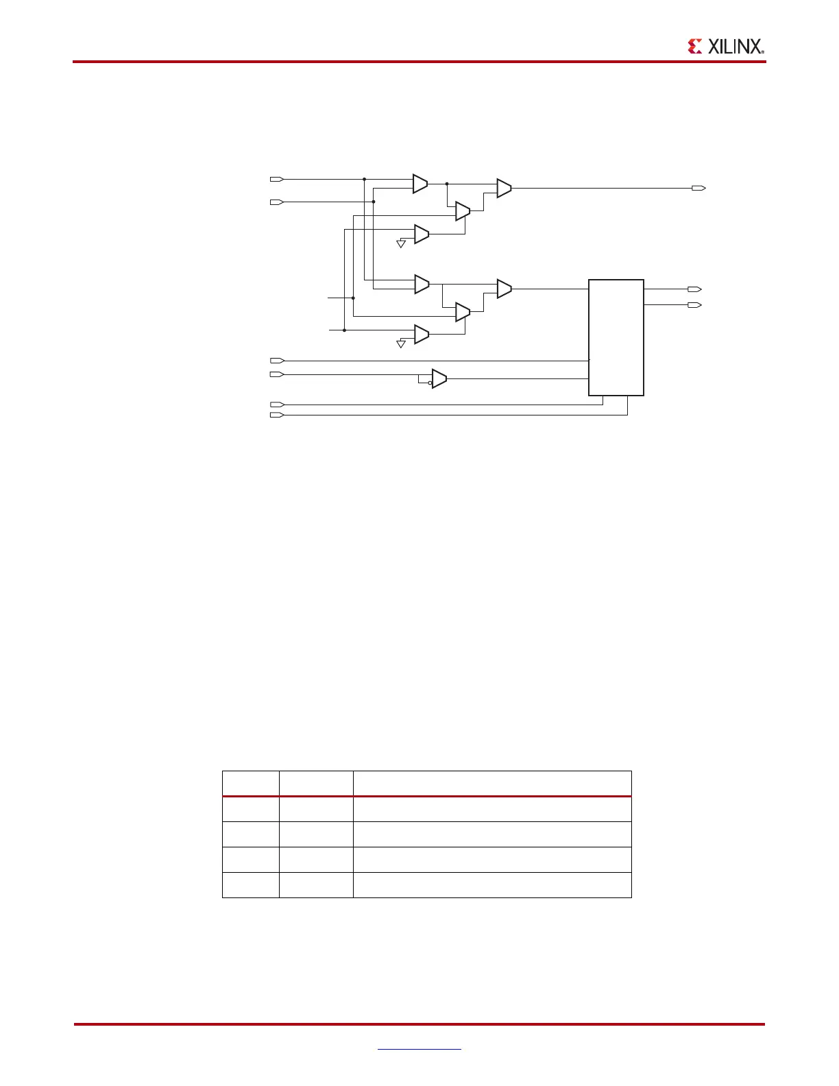
The ILOGIC block shown in Figure 7-1.
ILOGIC can support the following operations:
• Edge-triggered D-type flip-flop
• IDDR mode (OPPOSITE_EDGE or SAME_EDGE or SAME_EDGE_PIPELINED). See
“Input DDR Overview (IDDR),” page 319 for further discussion on input DDR.
• Level sensitive latch
• Asynchronous/combinatorial
All ILOGIC block registers have a common clock enable signal (CE1) that is active High by
default. If left unconnected, the clock enable pin for any storage element defaults to the
active state.
All ILOGIC block registers have a common synchronous or asynchronous set and reset (SR
and REV signals). The set/reset input pin, SR forces the storage element into the state
specified by the SRVAL attributes. When using SR, a second input, REV forces the storage
element into the opposite state. The reset condition predominates over the set condition.
Table 7-1 and Table 7-2 describe the operation of SR in conjunction with REV.
X-Ref Target - Figure 7-1
Figure 7-1: ILOGIC Block Diagram
Table 7-1: Truth Table when SRVAL = 0 (Default Condition)
SR REV Function
00NOP
0 1 Reset
10Set
1 1 Reset
D
DDLY
D
Q1
Q2
Q1
O
Q2
CE
CK
REVSR
CE1
CLK
SR
REV
ug190_7_01_050906
 Loading...


