322 www.xilinx.com Virtex-5 FPGA User Guide
UG190 (v5.0) June 19, 2009
Chapter 7: SelectIO Logic Resources
IDDR VHDL and Verilog Templates
The Libraries Guide includes templates for instantiation of the IDDR primitive in VHDL
and Verilog.
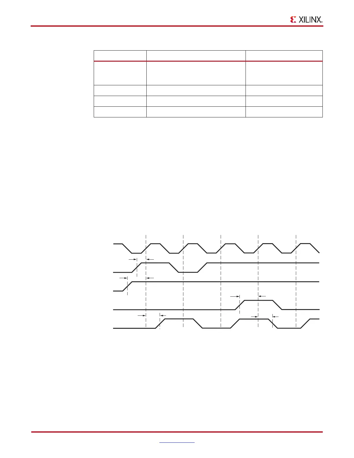
ILOGIC Timing Models
This section describes the timing associated with the various resources within the ILOGIC
block.
ILOGIC Timing Characteristics
Figure 7-6 illustrates ILOGIC register timing. When IDELAY is used, T
IDOCK
is replaced by
T
IDOCKD
.
Clock Event 1
• At time T
ICE1CK
before Clock Event 1, the input clock enable signal becomes valid-
High at the CE1 input of the input register, enabling the input register for incoming
data.
• At time T
IDOCK
before Clock Event 1, the input signal becomes valid-High at the D
input of the input register and is reflected on the Q1 output of the input register at
time T
ICKQ
after Clock Event 1.
Table 7-4: IDDR Attributes
Attribute Name Description Possible Values
DDR_CLK_EDGE Sets the IDDR mode of operation with
respect to clock edge
OPPOSITE_EDGE (default),
SAME_EDGE,
SAME_EDGE_PIPELINED
INIT_Q1 Sets the initial value for Q1 port 0 (default), 1
INIT_Q2 Sets the initial value for Q2 port 0 (default), 1
SRTYPE Set/Reset type with respect to clock (C) ASYNC (default), SYNC
X-Ref Target - Figure 7-6
Figure 7-6: ILOGIC Input Register Timing Characteristics
12345
CLK
D
CE1
SR
Q1
T
ICKQ
T
ICKQ
T
IDOCK
T
ICE1CK
T
ISRCK
ug190_7_06_041206
 Loading...


