364 www.xilinx.com Virtex-5 FPGA User Guide
UG190 (v5.0) June 19, 2009
Chapter 8: Advanced SelectIO Logic Resources
Timing Characteristics
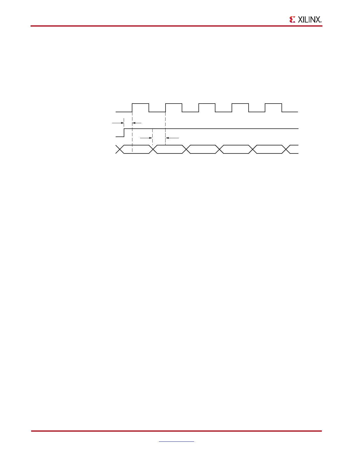
Figure 8-8 illustrates an ISERDES timing diagram for the input data to the ISERDES. The
timing parameter names change for different modes (SDR/DDR). However, the names do
not change when a different bus input width, including when two ISERDES are cascaded
together to form 10 bits. In DDR mode, the data input (D) switches at every CLK edge
(rising and falling).
Clock Event 1
• At time T
ISCCK_CE
, before Clock Event 1, the clock enable signal becomes valid-High
and the ISERDES can sample data.
Clock Event 2
• At time T
ISDCK_D
, before Clock Event 2, the input data pin (D) becomes valid and is
sampled at the next positive clock edge.
Reset Input Timing
Clock Event 1
As shown in Figure 8-9, the reset pulse is generated on the rising edge of CLKDIV. Because
the pulse must take two different routes to get to ISERDES0 and ISERDES1, there are
different propagation delays for both paths. The difference in propagation delay is
emphasized. The path to ISERDES0 is very long and the path to ISERDES1 is very short,
such that each ISERDES receives the reset pulse in a different CLK cycle. The internal resets
for both CLK and CLKDIV are reset asynchronously when the RST input is asserted.
X-Ref Target - Figure 8-8
Figure 8-8: ISERDES Input Data Timing Diagram
ug190_8_08_100307
CLK
CE
T
ISCCK_CE
T
ISDCK_D
12
D
 Loading...


