Virtex-5 FPGA User Guide www.xilinx.com 249
UG190 (v5.0) June 19, 2009
Specific Guidelines for I/O Supported Standards
GTLP (Gunning Transceiver Logic Plus)
The Gunning Transceiver Logic Plus, or GTL+ standard is a high-speed bus standard
(JESD8.3) first used by the Pentium Pro Processor. This standard requires a differential
amplifier input buffer and a open-drain output buffer. The negative terminal of the
differential input buffer is referenced to the V
REF
pin.
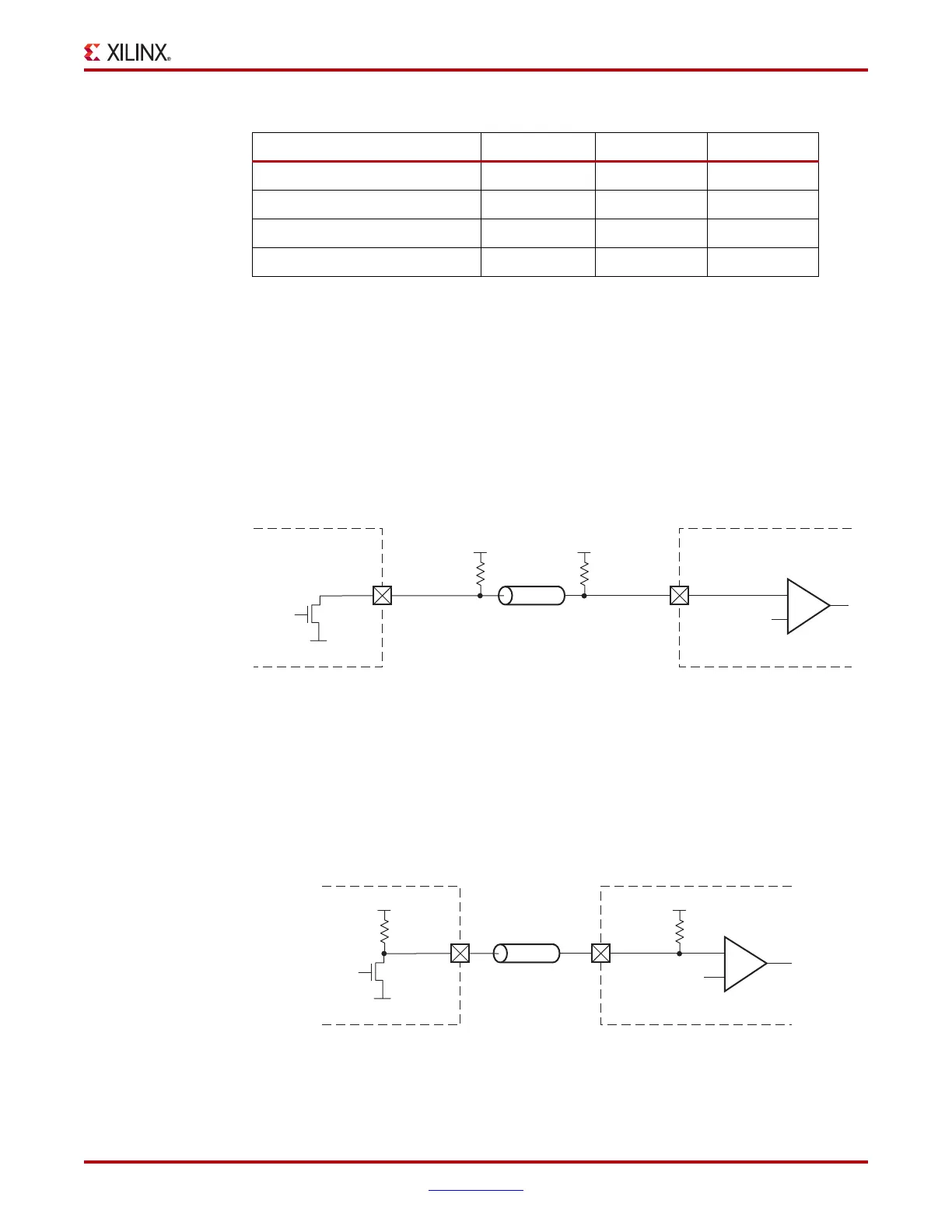
A sample circuit illustrating a valid termination technique for GTL+ with external parallel
termination and unconnected V
CCO
is shown in Figure 6-38.
GTLP_DCI Usage
GTL+ does not require a V
CCO
voltage. However, for GTLP_DCI, V
CCO
must be connected
to 1.5V. GTLP_DCI provides single termination to V
CCO
for inputs or outputs.
A sample circuit illustrating a valid termination technique for GTLP_DCI with internal
parallel driver and receiver termination is shown in Figure 6-39.
V
OL
– 0.2 0.4
I
OH
at V
OH
(mA) – – –
I
OL
at V
OL
(mA) at 0.4V 32 – –
I
OL
at V
OL
(mA) at 0.2V - – 40
Notes:
1. N must be greater than or equal to 0.653 and less than or equal to 0.68.
Table 6-13: GTL DC Voltage Specifications (Continued)
Parameter Min Typ Max
X-Ref Target - Figure 6-38
Figure 6-38: GTL+ with External Parallel Termination and Unconnected V
CCO
V
TT
= 1.5V
R
P
= Z
0
= 50Ω R
P
= Z
0
= 50Ω
V
CCO
= Unconnected
V
TT
= 1.5V
Z
0
= 50
IOB
IOB
ug190_6_36_030206
V
REF
= 1.0V
+
–
X-Ref Target - Figure 6-39
Figure 6-39: GTLP_DCI Internal Parallel Driver and Receiver Termination
V
CCO
= 1.5V
R
VRP
= Z
0
= 50Ω
50Ω
V
CCO
= 1.5V
Z
0
= 50
IOB
IOB
ug190_6_37_030206
V
REF
= 1.0V
+
–
 Loading...


