380 www.xilinx.com Virtex-5 FPGA User Guide
UG190 (v5.0) June 19, 2009
Chapter 8: Advanced SelectIO Logic Resources
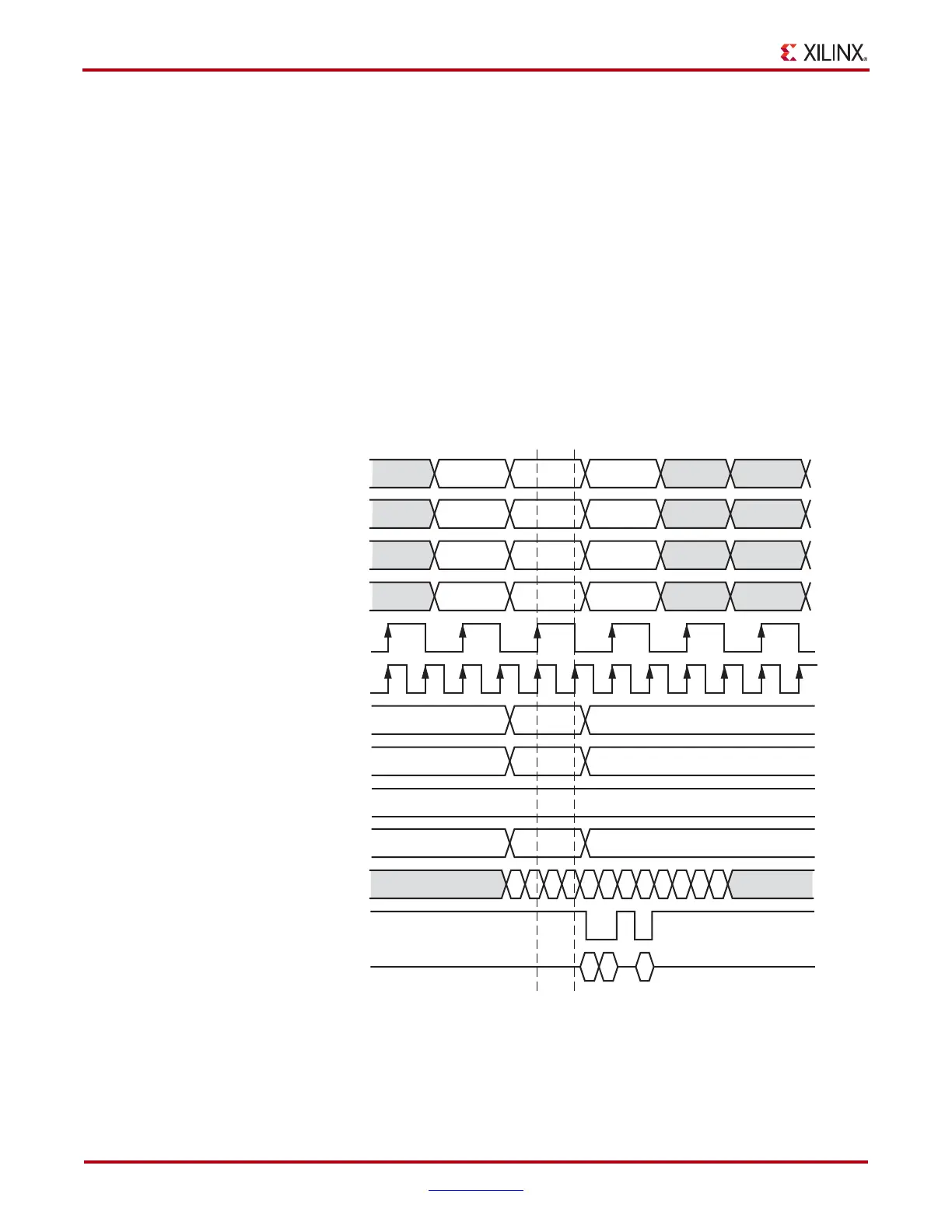
The second word IJKLMNOP is sampled into the master and slave OSERDES from the D1–
D6 and D3–D4 inputs, respectively.
Clock Event 4
Between Clock Events 3 and 4, the entire word ABCDEFGH is transmitted serially on OQ,
a total of eight bits transmitted in one CLKDIV cycle.
The data bit I appears at OQ four CLK cycles after IJKLMNOP is sampled into the
OSERDES. This latency is consistent with the Table 8-10 listing of a 8:1 DDR mode
OSERDES latency of four CLK cycles.
Timing Characteristics of 4:1 DDR 3-State Controller Serialization
The operation of a 3-State Controller is illustrated in Figure 8-19. The example is a 4:1 DDR
case shown in a bidirectional system where the IOB must be frequently 3-stated.
X-Ref Target - Figure 8-19
Figure 8-19: OSERDES Data Flow and Latency in 4:1 DDR Mode
Clock
Event 1
UG190_8_19_100307
D1 A E I
BFJ
CGK
D
10 1
10 1
111
1
AB CD EFGH
EF H
IJKL
01
HL
D2
D3
D4
CLKDIV
CLK
T1
T2
T3
T4
OQ
TQ
OBUFT.O
Clock
Event 2
 Loading...


