Virtex-5 FPGA User Guide www.xilinx.com 293
UG190 (v5.0) June 19, 2009
Specific Guidelines for I/O Supported Standards
Table 6-35 lists the differential SSTL (1.8V) Class II DC voltage specifications.
SSTL18_II_T_DCI (1.8V) Split-Thevenin Termination
Figure 6-86 shows a sample circuit illustrating a valid termination technique for
SSTL18_II_T_DCI (1.8V) with on-chip split-Thevenin termination. In this bidirectional I/O
standard, when 3-stated, the termination is invoked on the receiver and not on the driver.
Because the Thevenin termination on the I/O is disabled for a driving I/O, the line is
equivalent to the SSTL18_I termination scheme. This allows the line to be driven by the
weaker SSTL class I driver. The SSTL18_II_T_DCI standard behaves like a normal
SSTL18_II I/O in a bidirectional environment but has the advantage of lower drive
strength and lower power consumption due to the optimized termination circuit.
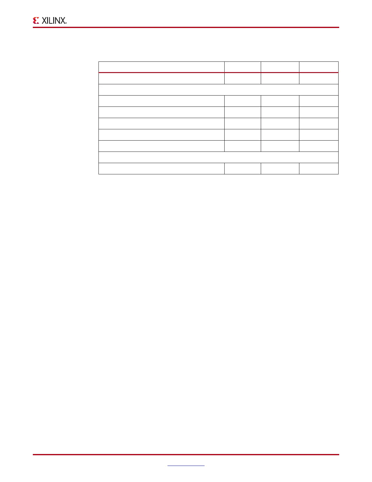
Table 6-35: Differential SSTL (1.8V) Class II DC Voltage Specifications
Min Typ Max
V
CCO
1.7 1.8 1.9
Input Parameters
V
TT
–V
CCO
× 0.5 –
V
IN
(DC)
(1)
–0.30 – V
CCO
+0.30
V
ID
(DC)
(3)
0.25 – V
CCO
+0.60
V
ID
(AC) 0.50 – V
CCO
+0.60
V
IX
(AC)
(4)
0.675 – 1.125
Output Parameters
V
OX
(AC)
(5)
0.725 – 1.075
Notes:
1. V
IN
(DC) specifies the allowable DC excursion of each differential input.
2. Per EIA/JESD8-6, “The value of V
REF
is to be selected by the user to provide optimum noise margin in
the use conditions specified by the user.”
3. V
ID
(DC) specifies the input differential voltage required for switching.
4. V
IX
(AC) indicates the voltage where the differential input signals must cross.
5. V
OX
(AC) indicates the voltage where the differential output signals must cross.
 Loading...


